


The SALORA 1G CHASSIS is a multi board multi modular chassis and it's quite complex.
The SALORA 1G CHASSIS is an awesome chassis since even higly advanced and complex it runs almost cool. That was even the reason why on front side was written "Low Energy Long Life".
The chassis was developing an excellent way to service each part:
All UNITS are easy to extract and put in simple position to perform any control or measurements.
Quality of materials is excellent even after many years is almost all like new.
The CHASSIS is divided by group of functions:
- Vertical Right Panel: Power supply + Line deflection + EHT + Frame deflection +
Synchronization.
The power supply is pretty unique since it introduces the concept of a unique transformer for all functions and its entirely developed by SALORA.
- Left Vertical panel: All signal processing + Video + Chroma + Audio + I.F. Video + I.F. Sound.
- Center little vertical panel: Tuning search and programs memory.
- Bottom horizontal boards: Remote control decoder + St-By supply.
The SALORA 1G CHASSIS is an awesome chassis even because higly advanced and complex it runs almost cool after many hours. That was even the reason why on front side was written "Low Energy Long Life"
(Lets see modern chinese crap build like this SALORA).
THE SALORA IPSALO (INTEGRATED POWER SUPPLY AND LINE OUTPUT) IN BRIEF:
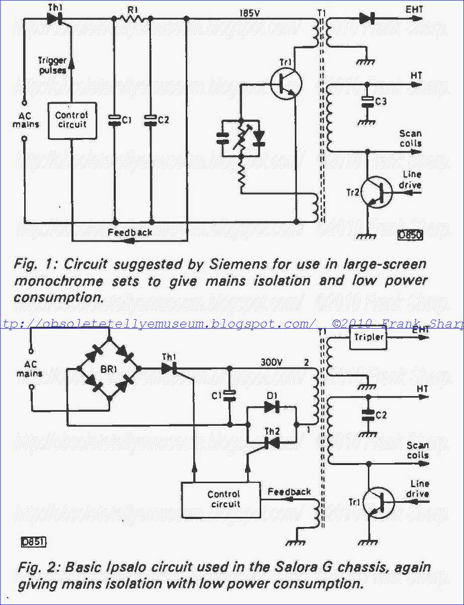 The
basic scheme is shown in Fig. 1, and as you can see this time we have
one transformer and two transistors, the single transformer providing
mains isolation in addition to being the line output/e.h.t. transformer.
The basic operation of this circuit is simple enough. Thl is a wholly
conventional thyristor rectifier producing a regulated h.t. supply. Cl
is the h.t. reservoir capacitor, with R1 and C2 the h.t. smoothing
components. R 1 also senses the h.t. current, feedback from the junction
of R1/C2 being taken to the control circuit to adjust the timing of the
trigger pulses used to fire Th 1. Transistor Tr 1 is a self
-oscillating chopper, driven by the flyback pulses applied to its base.
When it switches on, energy is fed into the transformer via its
collector winding. Those familiar with the Indesit T12 monochrome
portable and the GEC 3133/3135 portables will immediately recognise this
arrangement. The line output side is perfectly straightforward, with C3
smoothing the h.t. supply obtained at the top end of the line output
transistor's collector winding. One thing you could call this circuit is
"an inductive transfer system between the power supply and the line
timebase". Which brings us to the new Salora G chassis. Salora have
adopted this basic approach and taken it some stages further for use in
their new series G chassis, a mains/battery colour chassis designed to
drive 90° PIL type tubes in sizes up to 22in. Low power consumption is
obviously a prime requirement of a chassis that's to be able to do this,
so the circuit we've briefly described is an attractive starting point.
Salora call the circuit used in their G chassis "Ipsalo" - integrated
power supply and line output. The power consumption figures achieved
with the G chassis are certainly impressive - 38W with a 16in. tube and
45W with a 20 or 22in. tube, under normal viewing conditions. The Ipsalo
circuit is shown in greatly simplified form in Fig. 2. When operated
from the mains, bridge rectifier BR I will develop an h.t. supply of
300V across its reservoir capacitor C 1. It won't do this however until
Thl is switched on. Thl in fact is used for a totally different purpose
from Thl in Fig. 1. In this circuit both thyristors - Thl, and Th2 which
replaces Tr 1 in Fig. 1 - are switched at line frequency. Thl is used
as an electronic fuse, since with no drive the h.t. supply is removed.
It also provides the slow - start action. Th2 provides the regulation.
Th2 is switched on during the line scan period, being switched off by
the line flyback pulse which is coupled to it via the transformer. As
Salora point out, this is a much more economical way of switching it off
than the method used to switch off the scan thyristor in thyristor line
output circuits. Th2 is in fact being used as a chopper, with the shunt
diode D I providing an efficiency diode action. The scan/e.h.t. side of
the circuit is entirely conventional. Energy saving is achieved since
there is no electrical connection between the h.t. supply provided by
the thyristors and the line output stage, power transference being via
the magnetic fields produced by the current pulses flowing in winding
1-2 of the transformer. This minimises the dissipation in the set. The
control circuit that drives the thyristors is mainly contained in a 28
-pin thick -film hybrid i.c. (type LF0015) developed and manufactured by
Salora. In addition to driving the thyristors, it controls the soft
-start, electronic fusing and voltage limiting functions. Fig. 3 shows
the mains isolation arrangements in greater detail. The drives to both
thyristors are transformer coupled, while a further transformer (MM I)
feeds a second bridge rectifier from which the start-up supplies are
obtained. A further feed, via DB38, supplies a sample proportional to
the mains voltage to the control circuit.
The
basic scheme is shown in Fig. 1, and as you can see this time we have
one transformer and two transistors, the single transformer providing
mains isolation in addition to being the line output/e.h.t. transformer.
The basic operation of this circuit is simple enough. Thl is a wholly
conventional thyristor rectifier producing a regulated h.t. supply. Cl
is the h.t. reservoir capacitor, with R1 and C2 the h.t. smoothing
components. R 1 also senses the h.t. current, feedback from the junction
of R1/C2 being taken to the control circuit to adjust the timing of the
trigger pulses used to fire Th 1. Transistor Tr 1 is a self
-oscillating chopper, driven by the flyback pulses applied to its base.
When it switches on, energy is fed into the transformer via its
collector winding. Those familiar with the Indesit T12 monochrome
portable and the GEC 3133/3135 portables will immediately recognise this
arrangement. The line output side is perfectly straightforward, with C3
smoothing the h.t. supply obtained at the top end of the line output
transistor's collector winding. One thing you could call this circuit is
"an inductive transfer system between the power supply and the line
timebase". Which brings us to the new Salora G chassis. Salora have
adopted this basic approach and taken it some stages further for use in
their new series G chassis, a mains/battery colour chassis designed to
drive 90° PIL type tubes in sizes up to 22in. Low power consumption is
obviously a prime requirement of a chassis that's to be able to do this,
so the circuit we've briefly described is an attractive starting point.
Salora call the circuit used in their G chassis "Ipsalo" - integrated
power supply and line output. The power consumption figures achieved
with the G chassis are certainly impressive - 38W with a 16in. tube and
45W with a 20 or 22in. tube, under normal viewing conditions. The Ipsalo
circuit is shown in greatly simplified form in Fig. 2. When operated
from the mains, bridge rectifier BR I will develop an h.t. supply of
300V across its reservoir capacitor C 1. It won't do this however until
Thl is switched on. Thl in fact is used for a totally different purpose
from Thl in Fig. 1. In this circuit both thyristors - Thl, and Th2 which
replaces Tr 1 in Fig. 1 - are switched at line frequency. Thl is used
as an electronic fuse, since with no drive the h.t. supply is removed.
It also provides the slow - start action. Th2 provides the regulation.
Th2 is switched on during the line scan period, being switched off by
the line flyback pulse which is coupled to it via the transformer. As
Salora point out, this is a much more economical way of switching it off
than the method used to switch off the scan thyristor in thyristor line
output circuits. Th2 is in fact being used as a chopper, with the shunt
diode D I providing an efficiency diode action. The scan/e.h.t. side of
the circuit is entirely conventional. Energy saving is achieved since
there is no electrical connection between the h.t. supply provided by
the thyristors and the line output stage, power transference being via
the magnetic fields produced by the current pulses flowing in winding
1-2 of the transformer. This minimises the dissipation in the set. The
control circuit that drives the thyristors is mainly contained in a 28
-pin thick -film hybrid i.c. (type LF0015) developed and manufactured by
Salora. In addition to driving the thyristors, it controls the soft
-start, electronic fusing and voltage limiting functions. Fig. 3 shows
the mains isolation arrangements in greater detail. The drives to both
thyristors are transformer coupled, while a further transformer (MM I)
feeds a second bridge rectifier from which the start-up supplies are
obtained. A further feed, via DB38, supplies a sample proportional to
the mains voltage to the control circuit.
SALORA IPSALO CHASSIS 1G Regulated deflection system
SALORA 1GAH / SALORA CHASSIS 1G horizontal deflection circuit AND POWER SUPPLY:
SALORA-1G Regulated deflection circuit with start-up and electronic circuit breaker control:
Other References:
Bohringer et al., Laboratories RCA Ltd., Zurich, Switzerland, Reports MRZ 248, 3-23-79; MRZ 240E, 4-20-78.
Hollander, Laboratories, RCA Ltd., Zurich, Switzerland, Report MRZ 243, 11-15-78.
Dobbert, Electronic Circuit-Breaker with Surge Current Limiting for TV Receivers with a Thyristor Horizontal Deflection Stage, ITT Technical Report, 1-9-76.
A deflection generator develops scanning current in a deflection winding and produces a deflection rate alternating polarity voltage at a deflection generator terminal. A first winding of an input transformer is coupled to a source of supply frequency alternating polarity voltage and to a regulator switch for transferring energy from the source to a load circuit coupled to another winding of the input transformer. A second winding is coupled to the deflection generator terminal. The conduction time of the regulator switch controls the amount of energy transferred. A regulator control circuit turns on the regulator switch at a controlled instant within a first polarity interval of the deflection rate alternating polarity voltage to draw current in the first winding from the source. The deflection rate alternating polarity voltage applied to the second winding is reflected to the first winding and commutates off the regulator switch during the alternate polarity interval of each deflection cycle. A signal representative of variations in a deflection circuit energy level is applied to the regulator control circuit and varies the conduction time of the switch to regulate the energy level. A second controllable switch is coupled in the series path of the input current from the source of supply frequency alternating polarity voltage. A second control circuit generates a second switch turn-on signal to enable the input current to flow. During the start-up interval prior to steady-state operation of the deflection circuit, the second switch turn-on signal is generated immediately prior to the zero-crossover instants of the supply frequency alternating polarity voltage. Subsequently, the second switch turn-on signal is phase advanced from the zero-crossover instant to permit normal regulated deflection circuit operation to commence. 1. A regulated deflection circuit with start-up circuitry, comprising:
a deflection winding;
a deflection generator coupled to said deflection winding for generating scanning current in said deflection winding, a deflection rate voltage with an alternating polarity component voltage being developed at a deflection generator terminal;
a source of supply frequency alternating polarity voltage;
a controllable regulator switch;

an input transformer with first and second windings, said first winding being coupled to said source and to said regulator switch for transferring energy from said source to a load circuit coupled to a winding of said input transformer other than said first winding in accordance with the conduction time of said regulator switch, said second winding being coupled to said deflection generator terminal;
a regulator control circuit coupled to said regulator switch for turning on said regulator switch at a controlled instant within a first polarity interval of said deflection rate alternating polarity component voltage to draw current in said first winding from said source, said deflection rate alternating polarity component voltage being applied to said second winding for reflecting a resonant current to said first winding to commutate off said regulator switch during the alternate polarity interval;
means for developing a signal representative of variations of a deflection circuit energy level;
means for applying said deflection circuit energy level variations representative signal to said regulator control circuit to vary said conduction time of said regulator switch with deflection circuit energy level variations;
a second controllable switch coupled in the path of current from said source to said first winding of said input transformer;
a second control circuit coupled to said second switch for generating a second switch turn-on signal to enable current from said source to flow in said first winding of said input transformer;
means coupled to said second control circuit and responsive to said supply frequency alternating polarity voltage for enabling said second control circuit to generate said second switch turn-on signal at an instant prior to a zero-crossover instant within a cycle of said supply frequency alternating polarity voltage during deflection circuit start-up prior to steady-state operation; and
means for phase advancing the occurrence of said second switch turn-on signal from said zero-crossover instant during the transition from start-up to steady-state operation.

2. A circuit according to claim 1 including means for inhibiting the generation of said second switch turn-on signal for a predetermined inhibit interval upon initiation of deflection circuit start-up. 3. A circuit according to claim 2 including means responsive to said deflection rate voltage during steady-state operation of said deflection circuit for disabling generation of said second switch turn-on signal when sensing a decrease in amplitude of said deflection rate voltage below a predetermined level. 4. A circuit according to claim 3 including means for applying a deflection rate signal to said second control circuit during steady-state operation of said deflection circuit to generate said second switch turn-on signal within each cycle of said deflection rate voltage. 5. A circuit according to claim 3 wherein said inhibiting means comprises a flip-flop having two output state voltages, the first output state voltage when applied to said second control circuit inhibiting the generation of said second switch turn-on signal, the second output state voltage when applied enabling the generation of said second switch turn-on signal, said flip-flop developing said first output state voltage upon said initiation of deflection circuit start-up, and means for applying an input signal to said flip-flop to switch said flip-flop into developing said second output state voltage after the elapse of said predetermined inhibit interval. 6. A circuit according to claim 5 wherein said disabling means comprises means for applying an input signal to said flip-flop during steady-state operation of said deflection circuit when sensing a decrease in amplitude of said deflection rate voltage below said predetermined level such that said flip-flop switches into developing said first output state voltage. 7. A circuit according to any one of the preceding claims wherein said input transformer comprises a flyback transformer, said deflection rate voltage comprises a retrace pulse voltage, said first polarity interval comprises the trace interval of a deflection cycle and said alternate polarity interval comprises the retrace interval of a deflection cycle. 8. A circuit according to claim 7 wherein said first and second windings are loosely coupled to each other magnetically to provide sufficient leakage inductance to store within said flyback transformer the energy required to be transferred to said load circuit each deflection cycle. 9. A circuit according to claim 8 wherein said load circuit comprises an ultor load coupled to a high voltage winding of said flyback transformer, said high voltage winding and said second winding being relatively tightly coupled magnetically. 10. A circuit according to claim 9 wherein said regulator switch comprises a silicon controlled rectifier. 11. A circuit according to claim 10 including a rectifier parallelly coupled with and oppositely poled to said silicon controlled rectifier. 12. A circuit according to claim 11 wherein said second switch comprises a silicon controlled rectifier. 13. A regulated horizontal deflection circuit with start-up circuitry, comprising:
a horizontal deflection winding;
a trace capacitance for developing a trace voltage;
a horizontal deflection generator coupled to said deflection winding for applying said trace voltage to said deflection winding to generate scanning current in said deflection winding, a horizontal retrace pulse voltage being developed at a deflection generator terminal;
a source of mains supply alternating polarity voltage;
means coupled to said source for rectifying said mains supply voltage to develop a DC operating voltage at an input terminal;
a controllable regulator switch;
a DC blocking capacitance;

a flyback transformer with first and second windings, said first winding being coupled to said input terminal and to said regulator switch for transferring energy from said input terminal to a load circuit coupled to a winding of said flyback transformer other than said first winding in accordance with the conduction time of said regulator switch, said second winding being coupled to said deflection generator terminal and to said DC blocking capacitance;
a regulator control circuit coupled to said regulator switch for turning on said regulator switch at a controlled instant within the trace interval of each horizontal deflection cycle to draw current in said first winding from said input terminal, the horizontal retrace pulse voltage developed at said deflection generator terminal when applied to said second winding reflecting a resonant current to said first winding to commutate off said regulator switch during the retrace interval of each horizontal deflection cycle;
means for developing a signal representative of variations of a deflection circuit energy level;
means for applying said deflection circuit energy level variations representative signal to said regulator control circuit to vary said conduction time of said regulator switch with deflection circuit energy level variations;
a second controllable switch coupled in the path of the current from said source to said first winding of said flyback transformer;
a second control circuit coupled to said second switch for generating a second switch turn-on signal to enable current from said source to flow in said first winding;
means coupled to one of said trace and DC blocking capacitances for precharging said one capacitance to a predetermined level prior to the initial conduction of said regulator switch; and
means coupled to said second control circuit for enabling said second control circuit to generate said second switch turn-on signal near the zero-crossover instant of said mains supply voltage during deflection circuit start-up to provide a slow start-up of said deflection circuit.
14. A circuit according to claim 13 wherein said precharging means comprises an auxiliary mains supply transformer with a primary winding coupled to said source of mains supply alternating polarity voltage and including a rectifier coupled to said one capacitance and a secondary winding of said auxiliary mains supply transformer. 15. A circuit according to claim 14 including an audio load circuit coupled to a winding of said auxiliary mains supply transformer, said audio load circuit drawing an audio modulated load current from said mains supply source. 16. A circuit according to claims 13, 14 or 15 wherein said enabling means enables said second control circuit to generate said second switch turn-on signal at an instant immediately prior to said zero-crossover instant, said second control circuit including means for phase advancing the occurrence of said second switch turn-on signal from said zero-crossover instant during the transition from start-up to steady-state operation. 17. A circuit according to claim 16 including means responsive to said retrace pulse voltage during steady-state operation of said deflection circuit for disabling generation of said second switch turn-on signal when sensing a decrease in the amplitude of said retrace pulse voltage below a predetermined level.
Description:
This invention relates to regulated deflection circuits with start-up and electronic circuit breaker control.
 Switching regulators for television receiver power supplies may conveniently provide AC power line or mains supply isolation at the input transformer of the switching regulator. For regulator switches that are synchronized with horizontal deflection, the flyback transformer may provide mains supply isolation, with the flyback transformer functioning as the switching supply input transformer. The regulator switch is located in the nonisolated section of the power supply and is coupled in series with the primary winding of the flyback transformer across the mains supply source. The horizontal deflection generator including the horizontal deflection winding is coupled to a conductively isolated secondary winding of the flyback transformer.
The regulator switch is turned on at a controlled instant within the trace interval of each horizontal deflection cycle to draw input current in the flyback transformer primary winding from the mains supply. The energy stored in the flyback transformer during conduction of the regulator switch within the horizontal trace interval is transferred during retrace to secondary winding load circuits such as the horizontal deflection generator and the high voltage ultor load.
Several techniques are available for turning off the regulator switch during each horizontal deflection cycle. In one technique, a transistor is used as the regulator switch. A control circuit provides a reverse bias voltage to the base of the transistor, either towards the end of the trace interval or during the retrace interval, to turn the transistor off. Such a regulator circuit has the disadvantage of requiring a relatively complex control circuit to maintain the transistor conducting during trace and to turn off the transistor without undue dissipation in or damage to the device during turn-off.
In another technique, a thyristor such as a silicon controlled rectifier is used as the regulator switch. A relatively simple control circuit turns on the thyristor within the trace interval. An LC commutating circuit is coupled to the thyristor and initiates a resonant current oscillation upon thyristor turn-on. The thyristor is commutated off as the resonant current provided by the commutating circuit attempts to reverse direction in the thyristor. Such a circuit has the disadvantage of using a relatively costly inductor as part of the commutating circuit.
 In still another technique using a thyristor as a regulator switch, the thyristor is commutated off within the horizontal retrace interval by applying the retrace pulse voltage developed across the horizontal deflection winding to the secondary winding of the switching supply input flyback transformer. The retrace pulse voltage applied to the secondary winding of the flyback transformer reflects a resonant current to the primary winding to cause the current in the thyristor regulator switch to decrease during retrace until the thyristor is commutated off as the current therein attempts to reverse direction. An oppositely-poled diode may be coupled in parallel with the thyristor to return to the mains supply source any remaining energy stored in the flyback transformer after the thyristor is commutated off.
When using a thyristor as a regulator switch that is commutated off by a reflected retrace pulse, additional circuitry is desirable for slow start-up of the regulated deflection circuit and for electronic circuit breaker operation during overload and short-circuit conditions. A slow start mode of operation is desirable upon initial energization of the regulated deflection circuit because the retrace pulse voltage used to commutate off the thyristor switch is initially absent or of too low an amplitude. An electronic circuit breaker function is desirable to disable the regulator during short-circuit and overload conditions when the retrace pulse voltage is absent or unable to properly commutate off the regulator switch thyristor.
A feature of the invention is to provide slow or soft start regulator circuit operation by coupling a second controllable switch in the series path of the input current to the flyback transformer primary winding. During a first portion of the start-up interval after initial energization of the deflection circuit but prior to steady-state operation, the second controllable switch is turned on immediately prior to a zero-crossover instant within each cycle of the supply frequency alternating polarity or mains supply voltage. The second switch turn-on signals are then phase advanced from the zero-crossover instant during the transition from start-up to steady-state power supply and deflection circuit operation to enable greater amounts of input current to flow from the AC mains supply under normal steady-state deflection circuit operation.
A second feature of the invention is a circuit which inhibits the generation of the second switch turn-on signals for a predetermined interval upon initiation of the start-up interval. Such an inhibit interval is desirable to prevent transient voltages generated after the initial energization of the deflection circuit from improperly turning on the second switch at instants other than near the zero-crossover instant. In a specific embodiment, the output of a flip-flop having two output state voltages is applied to the control circuit of the second switch. Upon initiation of the start-up interval, the flip-flop develops the first output state voltage and inhibits the generation of the second switch turn-on signal. After the elapse of a predetermined interval from start-up initiation, the flip-flop changes output states and applies the second output voltage to the second switch control circuit to enable the generation of the second switch turn-on signal.
Another feature of the invention is to apply a deflection rate signal to the second switch control circuit during steady-state operation of the deflection circuit so as to generate the second switch turn-on signal during each cycle of horizontal deflection, thereby ensuring the turn-on of the second switch as soon as the mains supply voltage permits forward conduction through the switch.
Still another feature of the invention is to enable the second switch to function as an electronic circuit breaker to block the flow of input current from the mains supply during deflection circuit overload or short-circuit conditions during steady-state operation. A signal representative of the amplitude of the deflection rate voltage, such as a retrace pulse voltage, used to vary the regulator switch turn-on instant, is sensed by the electronic circuit breaker circuit. A sharp transition occurring in the sensed signal, which indicates that an overload or short-circuit condition has occurred, trips the circuit breaker. The inhibit flip-flop switches back to the first output state voltage, thereby preventing the second switch turn-on signal from being generated and thereby blocking the flow of input current.
Still another feature of the invention is to precharge the trace capacitor or the DC blocking capacitor that is coupled to the deflection generator coupled flyback transformer secondary winding. The trace or DC blocking capacitor is precharged prior to the initial conduction of the regulator switch so as to enable the generation of minimum amplitude retrace pulses for commutating off the regulator switch during start-up.
FIG. 1 illustrates a regulated deflection circuit with start-up and electronic circuit breaker control embodying the invention;
FIG. 2 illustrates waveforms associated with the operation of the circuit of FIG. 1;
FIG. 3 illustrates a portion of the circuit of FIG. 1 including detailed embodiments of the regulator, start-up and electronic circuit breaker circuits;
FIG. 4 illustrates the pin terminal connection of two conventional integrated circuits used when implementing the circuit of FIG. 3;
FIG. 5 illustrates waveforms associated with the operation of the circuit of FIG. 3; and
FIG. 6 illustrates a detailed embodiment of the low voltage power supply circuit portion of FIG. 1.
In a television receiver regulated horizontal deflection circuit 20, illustrated in FIG. 1, a source of supply frequency alternating polarity voltage 21, such as a 220 volt AC, 50 Hz, mains supply, is coupled across input terminals 22 and 23 of a full-wave bridge rectifier 26. A fuse 84 and a mechanical on-off switch 83 are coupled between source 21 and terminal 23. A terminal 25 of full-wave bridge rectifier 26 comprises the current return or earth ground terminal in common with the earth ground of mains supply 21. An output terminal 24 of full-wave bridge rectifier 26 is coupled through the anode-to-cathode path of a controllable switch, SCR 27, to an end terminal 28 of the primary winding 30a of an input transformer 30. A filter capacitor 29 is coupled to supply terminal 28 to develop a filtered but unregulated DC input voltage Vin at terminal 28. The other end terminal of input transformer winding 30a is coupled to the anode of a controllable regulator switch SCR 76. The cathode of SCR 76 is coupled to earth ground. Parallelly coupled with SCR 76, but oppositely poled, is a diode 77. SCR 76 and diode 77 may comprise a single semiconductor element 75 such as an integrated thyristor-rectifier (ITR).
Input transformer 30 may comprise a horizontal output or flyback transformer with a rectangular core 130. Primary winding 30a is wound around one leg of rectangular core 130 and secondary windings 30b-30d may be wound around the opposite leg. With the windings of flyback transformer 30 so situated, a substantial leakage inductance 230, due to loose magnetic coupling, exists between primary winding 30a and each of the secondary windings 30b-30d. By concentrically winding all of the secondary windings, for example, the secondary windings are relatively tightly coupled to each other magnetically and a relatively small leakage inductance exists between any two of the secondary windings.
An end terminal of flyback transformer secondary winding 30b is coupled to a horizontal deflection generator 48 at the collector of a horizontal output transistor 49. A DC blocking capacitor 47 is coupled to the other end terminal of secondary winding 30b. Horizontal deflection generator 48 comprises the series arrangement of a horizontal deflection winding 53 and an S-shaping or trace capacitor 52, a retrace capacitor 51, and a trace switch 54 comprising horizontal output transistor 49 and a damper diode 50. A conventional horizontal oscillator 55 provides a square-wave switching voltage 56, repeating at the horizontal deflection frequency, 1/T H , to a horizontal driver 57 for switching horizontal output transistor 49 into conduction within the horizontal trace interval of each deflection cycle and for cutting off the output transistor to initiate the horizontal retrace interval. A +15 volt DC supply voltage is applied to horizontal oscillator 55 at a terminal L and a +25 volt DC supply voltage is applied to horizontal driver 57 at a terminal M.
 The retrace pulse voltage Vr developed by deflection generator 48 at the collector of horizontal output transistor 49 is applied to flyback transformer secondary winding 30b, stepped up in voltage by high voltage secondary winding 30d, rectified by a diode 45 and filtered by a capacitor 46 to develop an ultor accelerating potential at a terminal U for the ultor load, not shown, of a television receiver picture tube. The retrace pulse voltage developed in flyback transformer secondary winding 30c is rectified by a diode 42 that is coupled to an end conductor lead 35 and filtered by a capacitor 43 to develop a +230 volt DC supply voltage at a terminal 44. The voltage developed across flyback transformer winding 30c is rectified during the trace interval by a diode 36 that is coupled to the other end conductor lead 31 and is filtered by a capacitor 37 to develop a +25 volt DC supply voltage at a terminal 38. A rectifier 39 is coupled to a tap terminal 32 of secondary winding 30c to develop a +15 volt DC supply voltage at a terminal 41 after filtering by a capacitor 40. A tap terminal 33 is coupled to a chassis ground conductively isolated from the mains supply earth ground.
A separate mains rectified auxiliary power supply 85, comprising an auxiliary mains supply transformer 62, a bridge rectifier 63, a diode 65 and a filter capacitor 66, provides +24 volts DC at a terminal 67. The +24 volts DC is used as a start-up supply, as will be explained, and also powers, for example, a high wattage audio circuit, not illustrated in FIG. 1.
During normal steady-state operation of deflection circuit 20, energy is transferred from mains supply 21 to the various load circuits coupled to the secondary windings of flyback transformer 30 including load circuits such as the ultor load and the horizontal deflection generator 48. Regulator SCR 76 is gated into conduction at a controlled instant within the trace interval of each horizontal deflection cycle by a gating pulse 78 developed by a regulator circuit 58. The gating pulse 78 is coupled by a transformer 60 to the gate of the SCR through a capacitor 70.
When SCR 76 is gated into conduction, a primary winding current i 1 flows in flyback transformer winding 30a and in SCR 76. To regulate a deflection circuit energy level, such as the retrace pulse amplitude Vr, the turn-on instant of SCR 76 and, thus, its conduction time, is varied by regulator control circuit 58 in response to variations of the deflection circuit energy level as represented by the retrace pulse 79 developed at a tap terminal 34 of secondary winding 30c and applied to the regulator control circuit along a conductor line 80. Operation of regulator circuit 58 is synchronized with horizontal deflection during start-up by applying to the regulator along a conductor line 81 the square-wave voltage 56 developed by horizontal oscillator 55, and is synchronized during steady-state operation by the applied retrace pulse 79.
 As illustrated in FIG. 2, the turn-on instant of regulator SCR 76 within the interval tla-tld is varied during the horizontal trace interval under varying load and mains supply voltage conditions to produce waveforms such as waveforms 71-74 representing the current i 1 flowing in primary winding 30a and ITR 75. The turn-on of SCR 76 varies from the instant tla for waveform 71 to the instant tld for waveform 74. In general, the current i 1 increases from the turn-on instant of the SCR until the instant t3 within the retrace interval is reached. The retrace pulse voltage Vr that is developed at the collector of horizontal output transistor 49 beginning at time t2 is applied to flyback transformer secondary winding 30b to reflect a resonating current to primary winding 30a such that the current i 1 in winding 30a begins to decrease in a resonant manner beginning at time t3. Near the center of the horizontal retrace interval, the current i 1 reverses direction and commutates off SCR 76. The negative current i 1 is then taken up by diode 77 to return energy to supply terminal 28. After termination of the retrace interval, the current i 1 agains flows as a positive-going but negatively-valued ramp until the zero current level is reached, at which time diode 77 is commutated off and the ITR becomes open-circuited.
Energy is transferred by way of flyback transformer 30 to the secondary winding coupled load circuits such as the ultor load during the horizontal retrace interval, as indicated by the peak magnitude of the positive current i 1 near the beginning of horizontal retrace being greater than the peak magnitude of the negative current near the end of horizontal retrace. The energy transferred during horizontal retrace is stored in the leakage inductance 230 of flyback transformer 30. Flyback transformer 30 is designed to provide sufficient leakage inductance to store all the required energy that is to be transferred under normal deflection circuit operation while still enabling the current i 1 to become negative during horizontal retrace in order to commutate off SCR 76. The amount of energy stored and transferred is a function of the conduction time of SCR 76 and ITR 75.
A feature of the invention is to ensure proper commutation of regulator SCR 76 during the start-up interval after closure of on-off switch 83 when the retrace pulse voltage Vr is absent or is of insufficient amplitude to reflect sufficient resonant current to primary winding 30a for commutation purposes. The start-up circuit for deflection circuit 20 includes SCR 27 and a control circuit 59 for providing turn-on gating pulses to SCR 27 by way of a transformer 61 and a capacitor 69.
DC blocking capacitor 47 and trace capacitor 52 are precharged through a diode 68 from the 24 volt supply terminal 67 of auxiliary supply 85 prior to the initial conduction of regulator SCR 76. This precharging enables the immediate generation of relatively low amplitude retrace pulses Vr when horizontal oscillator 55 begins to provide the square-wave switching voltage 56. The current i 1 in primary winding 30a is maintained at a relatively small value in order to permit the low amplitude retrace pulse voltage Vr during start-up to commutate off regulator SCR 76.
To maintain a low amplitude to the current i 1 during start-up, the input voltage Vin is made to increase relatively slowly during the start-up interval. SCR 27 is coupled in the series circuit path for input current from the AC mains supply 21 to primary winding 30a. Control circuit 59 initially provides gating pulses to SCR 27 immediately prior to the zero-crossover instants of the alternating polarity mains supply voltage. To synchronize operation of control circuit 59 with the alternating polarity mains supply voltage, the full-wave rectified mains voltage V 64 , repeating at twice the mains supply frequency f AC , is applied to control circuit 59 from terminal 64 along a conductor line 82.
By turning on SCR 27 immediately prior to the zero-crossover instants of the mains supply voltage, the conduction time of SCR 27 is kept relatively short. A relatively small amount of input current flows from mains supply 21, resulting in a relatively low input voltage Vin being developed at terminal 28 and a relatively small current i 1 flowing in primary winding 30a. SCR 76 can therefore be commutated off during the start-up interval when the retrace pulse voltage amplitude is relatively small. Control circuit 59 then phase advances the gating of SCR 27 away from the zero-crossover instants during the transition from start-up to steady-state operation to enable greater amounts of input current to flow and to bring up the input voltage Vin to its steady-state value.
Another feature of the invention is to combine an electronic circuit breaker function with the start-up function of SCR 27. If a flyback transformer secondary winding coupled load, such as the ultor load, short circuits and substantially reduces the amplitude of the retrace pulse voltage Vr, or if, for example, deflection generator 48 malfunctions and fails to generate a retrace pulse voltage, regulator SCR 76 will not be commutated off. To prevent the current i 1 in flyback transformer primary winding 30a from increasing to prohibitive values under a short-circuited secondary load condition or a malfunctioning deflection generator condition, a retrace pulse voltage 79 is applied to control circuit 59 along conductor line 80. Control circuit 59 prevents the generation of gating pulses to SCR 27 when sensing a negative-going transient produced by the collapse of retrace pulse voltage 79. The input current path to primary winding 30a from mains supply 21 is then opened up, thereby disabling normal deflection circuit operation.
After normal deflection circuit operation is disabled, the start-up portion of control circuit 59 again turns on SCR 27 immediately prior to the zero-crossover instants of the mains supply voltage to repeat the slow start sequence. Should the fault condition persist, the disabling circuit portion of control circuit 59 will again be activated to disable deflection circuit 20. Operation of deflection circuit 20 under a persistent fault condition will cycle between start-up and disabling modes of operation until fuse 84 opens up and maintains the deflection circuit disabled.
During the steady-state operation of deflection circuit 20, control circuit 59 applies a gating pulse to SCR 27 once each horizontal deflection cycle in response to the horizontal deflection rate square-wave voltage 56 applied to control circuit 59 along conductor line 81. By providing a turn-on gating signal to SCR 27 each deflection cycle, conduction of the SCR is assured as soon as the anode potential of the SCR exceeds the cathode potential.
 FIG. 3 illustrates a portion of the circuit of FIG. 1 including detailed embodiments of regulator control circuit 58 and the start-up and electronic circuit breaker control circuit 59. A 15 volt DC voltage at terminal L and a 6.8 volt DC voltage at a terminal N provide supply rail operating voltages for the two control circuits.
Under normal, steady-state deflection circuit operation, a driver transistor Q5 within regulator control circuit 58 is switched on at a controlled instant within the trace interval of each deflection cycle to produce gating pulses 78 to turn on regulator SCR 76. The exact turn-on instant of transistor Q5 is determined by the triggering of a comparator 90 in accordance with variations in the amplitude of retrace pulse 79 applied to regulator control circuit 58 along conductor line 80.
During the start-up interval, after closure of on-off switch 83, comparator 90 is triggered by the leading or positive-going edge of the horizontal deflection rate square-wave voltage 56 obtained from horizontal oscillator 55 and applied to input pin 5 of comparator 90 after first being differentiated. The leading edge of square-wave voltage 56 is also used to turn off horizontal output transistor 49. Thus, during start-up, the turn-on of regulator SCR 76 occurs near the end of the horizontal trace interval.
As the deflection current steadily increases during the start-up interval, the amplitude of the horizontal retrace pulses 79 applied along conductor line 80 also increases. A horizontal rate sawtooth voltage is developed at input pin 6 of comparator 90. This sawtooth voltage is obtained by the integration of flyback pulses 79 by resistor R3 and capacitor C5 after being square-wave shaped by a zener diode D6. The sawtooth voltage at pin 6 of comparator 90 advances the triggering of the comparator and the turn-on of SCR 76 relative to the turn-on instant produced by the leading edge of square-wave voltage 56. SCR 76 gradually conducts longer, and increasingly greater amounts of energy are transferred to the flyback transformer secondary winding coupled load circuits until a steady-state equilibrium condition has been achieved.
During steady-state operation, a diode D4 rectifies retrace pulse 79 to produce a DC control voltage at a terminal E across a capacitor C4. The DC control voltage varies with retrace pulse amplitude variations. The DC control voltage is level shifted by a zener diode D5 and combined with the sawtooth voltage at pin 6 of comparator 90 to vary the triggering of comparator 90 and the turn-on of SCR 76 so as to maintain the retrace pulse voltage amplitude relatively constant.
 To provide for the slow increase in the input voltage Vin, start-up control circuit 59 initially turns on SCR 27 immediately prior to the zero-crossover instants of the mains supply voltage. The full-wave rectified mains supply voltage V 64 , illustrated in FIG. 5a, is applied to an input pin 4 of a comparator 92. Comparator 92 inverts and limits the rectified mains supply voltage to produce a square-wave voltage V A , illustrated in FIG. 5b, at a terminal A, the output pin 2 of comparator 92. The positive portion of square-wave voltage V A occurs between times t 1 -t 4 encompassing the zero-crossover instant t 3 of the full-wave rectified mains supply voltage V 64 .
Square-wave voltage V A is differentiated by a capacitor 88 and a resistor 89 to produce the voltage V B across resistor 89 at a terminal B, as illustrated in FIG. 5c. The negative differentiated spike portion of the voltage V B occurring at the trailing edge of the square-wave voltage V A at time t 4 is applied to an input pin 6 of a monostable 93, at a terminal C. The voltage at pin 6 of monostable 93 is square-wave shaped by a diode D1 to produce the negative pulse voltage V D1 at time t 4 , illustrated in FIG. 5d. The negative-going edge of the pulse V D1 causes the monostable to switch output state voltages at output pin 1, at a terminal D. As illustrated in FIG. 5e, the voltage V D at terminal D goes high at time t 4 .
The output of monostable 93 remains high for a predetermined interval t 4 -t 8 of FIG. 5e. The duration t 4 -t 8 of the unstable high output state of monostable 93 is determined by the voltage V C1 developed at input pin 6 of monostable 93 after the occurrence of the negative pulse V D1 , as illustrated in FIGS. 5d and 5e. During the occurrence of the first several gating pulses for SCR 27, the voltage at pin 6 of monostable 93 is determined by the values of voltage dividing resistors 96 and 97 in parallel with resistor 128. These values are selected to enable monostable 93 to switch back to its stable low state at the instant t 2 or t 8 , an instant immediately prior to the zero-crossover instant t 3 or t 9 of the voltage V 64 , as illustrated in FIGS. 5a and 5e.
The negative-going edge at time t 2 or t 8 of the resultant square-wave output voltage V D of monostable 93 is differentiated by the network 120-125 to apply a negative spike voltage 98 to the base of a driver transistor Q4 to turn the transistor on, as illustrated by the base voltage V bQ4 and by the collector voltage V cQ4 of FIGS. 5f and 5g. The resulant pulsed collector voltage comprises the gating pulses 179 of FIG. 5g. Pulses 179 are applied through transformer 61 to turn on SCR 27 at times t 2 and t 8 immediately prior to zero-crossover instants t 3 and t 9 of the full-wave rectified AC mains voltage V 64 , as required to provide slow start-up operation of deflection circuit 20.
Upon initial energization of horizontal deflection circuit 20 of FIG. 1, when on-off switch 83 is closed, undesirable transient voltages may be developed which can spuriously trigger SCR 27 at instants other than near the zero-crossover instants of the mains supply voltage. An inhibit circuit 126, illustrated in FIG. 3, is included in the control circuit 59 of SCR 27. Inhibit circuit 126 disables the output of monostable 93, thereby preventing transistor Q4 from turning on and triggering SCR 27. Inhibit circuit 126 is activated for a predetermined interval, typically around 0.5 to 1 second. After the elapse of this inhibit interval, the output of monostable 93 is no longer disabled, thereby permitting the triggering of SCR 27 immediately prior to a zero-crossover instant of the mains supply voltage.
Inhibit circuit 126 comprises a flip-flop 95 having an output pin 14 coupled to the output path of monostable 93 by way of a diode D3. Immediately after closure of on-off switch 83, the output of flip-flop 95 is low or grounded, thereby grounding terminal F which is coupled to the anode of diode D3. SCR 27 cannot be triggered as long as output pin 14 of flip-flop 95 is in the ground state.
After approximately 0.8 second, as determined by the time constant of a resistor R2 and a capacitor C3, capacitor C3 has charged sufficiently to raise the voltage at input pin 9 of flip-flop 95 to a value that will cause flip-flop 95 to change output states at pin 14. Diode D3 becomes reverse biased and the output of monostable 93 is now permitted to turn on transistor Q4 and trigger SCR 27.
During the 0.8 second inhibit interval when the output pin 14 of flip-flop 95 is grounded, a capacitor C2, coupled to output pin 14 through a diode 127, is maintained in a discharged state. After the elapse of the inhibit interval, output pin 14 goes high, reverse biasing diode 127 and permitting capacitor C2 to charge from the 6.8 volt supply rail through a resistor R1. The increasing voltage across capacitor C2 is applied to input pin 6 of monostable 93 through a diode D2 and a resistor 128. Since the duration of the unstable high output state of monostable 93 is a function of the voltage V C at pin 6 of monostable 93, increasing the voltage V C by charging capacitor C2 results in the shortening of the unstable high output state at terminal D.
As illustrated in FIG. 5d, as capacitor C2 charges, the voltage V C at pin 6 of monostable 93 continuously increases from the value V C1 to the value V C2 and then to the value V C3 . As illustrated in FIGS. 5e and 5g, because of the increasing voltage applied by capacitor C2 to input pin 6 of monostable 93, the duration of the unstable high state of monostable 93 shortens. The output of monostable 93 returns to its stable low state at a continuously advancing instant such as the advanced instant t 6 and then the advanced instant t 5 , resulting in the continuous phase advance of the triggering of SCR 27 away from near the zero-crossover instant to the instant t 6 , for example, and then to the instant t 5 .
As the triggering instant of SCR 27 phase advances, increasingly greater amounts of input current flow from mains supply 21 through SCR 27 to charge capacitor 29 to provide a slowly increasing voltage Vin, as is required for soft start-up operation of deflection circuit 20.
As the input voltage Vin approaches its steady-state level, a trigger comparator 91 is enabled and switches transistor Q4 into conduction each horizontal deflection cycle to trigger SCR 25 into conduction each deflection cycle. An output pin 1 of comparator 91 is coupled to the base of transistor Q4 through a resistor 129. The horizontal deflection rate square-wave switching voltage 56 is applied to the positive input pin terminal 3 of comparator 91 along conductor line 81. The increasing voltage developed across capacitor C2 is applied to the inverting input pin 2 of comparator 91.
As the voltage across capacitor C2 reaches its steady-state level, the voltage applied to inverting pin 2 of comparator 91 is sufficiently great to trigger the comparator into the low output state upon the occurrence of the negative-going edge of the horizontal deflection rate square-wave voltage 56. When the output of comparator 91 goes low, transistor Q4 is turned on, thereby triggering SCR 27 into conduction. Triggering SCR 27 at a horizontal rate as steady-state conditions are approached ensures the optimal triggering of the SCR as soon as the full-wave rectified mains supply voltage V 64 applied to the anode of SCR 27 exceeds the SCR cathode potential.
The low voltage power supply 180 of FIG. 1 provides +15 volts DC and +25 volts DC at terminals L and M, respectively, for energizing horizontal oscillator 55, horizontal driver 57, regulator 58 and start-up and electronic circuit breaker 59 during start-up. Power supply 180 also provides +6.8 volts DC at terminal N for energizing circuits 58 and 59 both during start-up and steady-state operation.
 A detailed embodiment of power supply 180 is illustrated in FIG. 6. A zener diode 86 maintains the voltage at terminal N at +6.8 volts DC. Zener bias is obtained through a resistor 87 from the +24 volts DC at terminal 67 developed by auxiliary power supply 85.
During start-up, the +24 volts at terminal 67 is applied to terminal M through a resistor 181 and a diode 182. The start-up voltage at terminal M, although less than the steady-state terminal M voltage of +25 volts DC, is sufficient to energize horizontal driver 57 into operation. During steady-state operation, flyback transformer 30 of FIG. 1 provides +25 volts DC at terminal M of FIG. 6 through terminal 38 and a diode 183. During steady-state operation, diode 182 is reverse biased, disconnecting auxiliary power supply 85 from terminal M.
Also, during start-up, the +24 volts at terminal 67 is applied to terminal L through resistor 181, a transistor 184 and a diode 185. The start-up voltage at terminal L, although less than the steady-state terminal L voltage of +15 volts DC, is sufficient to energize horizontal oscillator 55, regulator 58 and start-up and electronic circuit breaker 59 into operation. During steady-state operation, the flyback transformer derived voltage of +15 volts DC developed at terminal 41 is applied through a diode 186 to reverse bias diode 185 and to establish the +15 volts steady-state DC voltage at terminal L.
As indicated previously, the +24 volts DC at terminal 67 power a high wattage audio circuit, illustrated in FIG. 6 as the audio circuit 190. Audio circuit 190 comprises an audio amplifier 192 with an output terminal AC coupled through a capacitor 193 to the primary winding of a coupling transformer 194. The secondary winding of transformer 194 is coupled to the voice coil 195 of a loudspeaker 196. Audio frequency signals are applied to input terminal 191 of audio amplifier 192. These signals are amplified by audio amplifier 192 to generate current in voice coil 195, thereby producing sound emanations from loudspeaker 196 in accordance with the sound information content of the signals.
Audio load circuit 190 may be a relatively high wattage load, consuming, illustratively, 10-20 watts power. If audio load circuit 190 were to draw its load current from a flyback transformer secondary winding supply voltage, such as from terminal 38, substantial undesirable retrace pulse voltage modulation may occur due to variations in load current being drawn from the flyback transformer secondary winding. These load current variations may be the result of sound content changes in the audio input signals applied to terminal 191. To avoid undesirable audio retrace pulse modulation, the +24 volt DC supply is provided by the same auxiliary power supply 85 as is used to precharge DC blocking capacitor 47. The audio load current is now drawn from the mains supply source through auxiliary transformer 62 rather than through flyback transformer 30.
Short-circuit, overload and deflection generator malfunction protection is provided by a shutdown circuit 130 incorporated into the control circuit 59 of SCR 27 and illustrated in FIG. 3. A trigger comparator 94 has its output pin 13 coupled to input pin 8 of flip-flop 95. The inverting input pin 10 of trigger comparator 94 is coupled through a capacitor 131 to terminal E. The voltage at terminal E represents the rectified retrace pulse voltage amplitude.
If the regulator ITR 75 short circuits, or if the ultor load short circuits due to picture tube arcing, or if deflection generator 48 malfunctions and fails to produce retrace pulse voltages, the voltage at terminal E decreases to zero. Trigger comparator 94 senses the collapsing voltage at terminal E and switches to the high output state, thereby triggering flip-flop 95 into the low output state. When the output of flip-flop 95 is low or grounded, capacitor C2 is discharged, disabling the operation of both monostable 93 and trigger comparator 91. Transistor Q4 cannot be turned on, thereby removing trigger pulses from SCR 27 and maintaining the SCR in the off state. The input voltage Vin is removed, thereby disabling and shutting down operation of horizontal deflection circuit 20. After shutdown, the start-up sequence for horizontal deflection circuit 20 is reinitiated. If the fault condition persists, shutdown will again occur and eventually fuse 84 will open.
 Comparators 90-92 and 94, monostable 93 and flip-flop 95 may be obtained from conventional integrated circuit packages. As illustrated in FIG. 4, comparators 90 and 91 may be obtained from the integrated circuit package CA393, manufactured by RCA Corporation, Somerville, N.J., or from the package LM393, manufacture by National Semiconductor Corporation, Santa Clara, Calif., with the output pins connected as indicated in FIGS. 3 and 4. Comparators 92 and 94, monostable 93, and flip-flop 95 may be obtained from the integrated circuit package CA339, manufactured by RCA Corporation, or from the package LM339, manufactured by National Semiconductor Corporation.
The regulator switch is turned on at a controlled instant within the trace interval of each horizontal deflection cycle to draw input current in the flyback transformer primary winding from the mains supply. The energy stored in the flyback transformer during conduction of the regulator switch within the horizontal trace interval is transferred during retrace to secondary winding load circuits such as the horizontal deflection generator and the high voltage ultor load.
Several techniques are available for turning off the regulator switch during each horizontal deflection cycle. In one technique, a transistor is used as the regulator switch. A control circuit provides a reverse bias voltage to the base of the transistor, either towards the end of the trace interval or during the retrace interval, to turn the transistor off. Such a regulator circuit has the disadvantage of requiring a relatively complex control circuit to maintain the transistor conducting during trace and to turn off the transistor without undue dissipation in or damage to the device during turn-off.
In another technique, a thyristor such as a silicon controlled rectifier is used as the regulator switch. A relatively simple control circuit turns on the thyristor within the trace interval. An LC commutating circuit is coupled to the thyristor and initiates a resonant current oscillation upon thyristor turn-on. The thyristor is commutated off as the resonant current provided by the commutating circuit attempts to reverse direction in the thyristor. Such a circuit has the disadvantage of using a relatively costly inductor as part of the commutating circuit.
In still another technique using a thyristor as a regulator switch, the thyristor is commutated off within the horizontal retrace interval by applying the retrace pulse voltage developed across the horizontal deflection winding to the secondary winding of the switching supply input flyback transformer. The retrace pulse voltage applied to the secondary winding of the flyback transformer reflects a resonant current to the primary winding to cause the current in the thyristor regulator switch to decrease during retrace until the thyristor is commutated off as the current therein attempts to reverse direction. An oppositely-poled diode may be coupled in parallel with the thyristor to return to the mains supply source any remaining energy stored in the flyback transformer after the thyristor is commutated off. When using a thyristor as a regulator switch that is commutated off by a reflected retrace pulse, additional circuitry is desirable for slow start-up of the regulated deflection circuit and for electronic circuit breaker operation during overload and short-circuit conditions. A slow start mode of operation is desirable upon initial energization of the regulated deflection circuit because the retrace pulse voltage used to commutate off the thyristor switch is initially absent or of too low an amplitude. An electronic circuit breaker function is desirable to disable the regulator during short-circuit and overload conditions when the retrace pulse voltage is absent or unable to properly commutate off the regulator switch thyristor.
A feature of the invention is to provide slow or soft start regulator circuit operation by coupling a second controllable switch in the series path of the input current to the flyback transformer primary winding. During a first portion of the start-up interval after initial energization of the deflection circuit but prior to steady-state operation, the second controllable switch is turned on immediately prior to a zero-crossover instant within each cycle of the supply frequency alternating polarity or mains supply voltage. The second switch turn-on signals are then phase advanced from the zero-crossover instant during the transition from start-up to steady-state power supply and deflection circuit operation to enable greater amounts of input current to flow from the AC mains supply under normal steady-state deflection circuit operation.
A second feature of the invention is a circuit which inhibits the generation of the second switch turn-on signals for a predetermined interval upon initiation of the start-up interval. Such an inhibit interval is desirable to prevent transient voltages generated after the initial energization of the deflection circuit from improperly turning on the second switch at instants other than near the zero-crossover instant. In a specific embodiment, the output of a flip-flop having two output state voltages is applied to the control circuit of the second switch. Upon initiation of the start-up interval, the flip-flop develops the first output state voltage and inhibits the generation of the second switch turn-on signal. After the elapse of a predetermined interval from start-up initiation, the flip-flop changes output states and applies the second output voltage to the second switch control circuit to enable the generation of the second switch turn-on signal.
Another feature of the invention is to apply a deflection rate signal to the second switch control circuit during steady-state operation of the deflection circuit so as to generate the second switch turn-on signal during each cycle of horizontal deflection, thereby ensuring the turn-on of the second switch as soon as the mains supply voltage permits forward conduction through the switch.
Still another feature of the invention is to enable the second switch to function as an electronic circuit breaker to block the flow of input current from the mains supply during deflection circuit overload or short-circuit conditions during steady-state operation. A signal representative of the amplitude of the deflection rate voltage, such as a retrace pulse voltage, used to vary the regulator switch turn-on instant, is sensed by the electronic circuit breaker circuit. A sharp transition occurring in the sensed signal, which indicates that an overload or short-circuit condition has occurred, trips the circuit breaker. The inhibit flip-flop switches back to the first output state voltage, thereby preventing the second switch turn-on signal from being generated and thereby blocking the flow of input current.
Still another feature of the invention is to precharge the trace capacitor or the DC blocking capacitor that is coupled to the deflection generator coupled flyback transformer secondary winding. The trace or DC blocking capacitor is precharged prior to the initial conduction of the regulator switch so as to enable the generation of minimum amplitude retrace pulses for commutating off the regulator switch during start-up.
FIG. 1 illustrates a regulated deflection circuit with start-up and electronic circuit breaker control embodying the invention;
FIG. 2 illustrates waveforms associated with the operation of the circuit of FIG. 1;
FIG. 3 illustrates a portion of the circuit of FIG. 1 including detailed embodiments of the regulator, start-up and electronic circuit breaker circuits;
FIG. 4 illustrates the pin terminal connection of two conventional integrated circuits used when implementing the circuit of FIG. 3;
FIG. 5 illustrates waveforms associated with the operation of the circuit of FIG. 3; and
FIG. 6 illustrates a detailed embodiment of the low voltage power supply circuit portion of FIG. 1.
In a television receiver regulated horizontal deflection circuit 20, illustrated in FIG. 1, a source of supply frequency alternating polarity voltage 21, such as a 220 volt AC, 50 Hz, mains supply, is coupled across input terminals 22 and 23 of a full-wave bridge rectifier 26. A fuse 84 and a mechanical on-off switch 83 are coupled between source 21 and terminal 23. A terminal 25 of full-wave bridge rectifier 26 comprises the current return or earth ground terminal in common with the earth ground of mains supply 21. An output terminal 24 of full-wave bridge rectifier 26 is coupled through the anode-to-cathode path of a controllable switch, SCR 27, to an end terminal 28 of the primary winding 30a of an input transformer 30. A filter capacitor 29 is coupled to supply terminal 28 to develop a filtered but unregulated DC input voltage Vin at terminal 28. The other end terminal of input transformer winding 30a is coupled to the anode of a controllable regulator switch SCR 76. The cathode of SCR 76 is coupled to earth ground. Parallelly coupled with SCR 76, but oppositely poled, is a diode 77. SCR 76 and diode 77 may comprise a single semiconductor element 75 such as an integrated thyristor-rectifier (ITR). Input transformer 30 may comprise a horizontal output or flyback transformer with a rectangular core 130. Primary winding 30a is wound around one leg of rectangular core 130 and secondary windings 30b-30d may be wound around the opposite leg. With the windings of flyback transformer 30 so situated, a substantial leakage inductance 230, due to loose magnetic coupling, exists between primary winding 30a and each of the secondary windings 30b-30d. By concentrically winding all of the secondary windings, for example, the secondary windings are relatively tightly coupled to each other magnetically and a relatively small leakage inductance exists between any two of the secondary windings.
An end terminal of flyback transformer secondary winding 30b is coupled to a horizontal deflection generator 48 at the collector of a horizontal output transistor 49. A DC blocking capacitor 47 is coupled to the other end terminal of secondary winding 30b. Horizontal deflection generator 48 comprises the series arrangement of a horizontal deflection winding 53 and an S-shaping or trace capacitor 52, a retrace capacitor 51, and a trace switch 54 comprising horizontal output transistor 49 and a damper diode 50. A conventional horizontal oscillator 55 provides a square-wave switching voltage 56, repeating at the horizontal deflection frequency, 1/T H , to a horizontal driver 57 for switching horizontal output transistor 49 into conduction within the horizontal trace interval of each deflection cycle and for cutting off the output transistor to initiate the horizontal retrace interval. A +15 volt DC supply voltage is applied to horizontal oscillator 55 at a terminal L and a +25 volt DC supply voltage is applied to horizontal driver 57 at a terminal M.
A separate mains rectified auxiliary power supply 85, comprising an auxiliary mains supply transformer 62, a bridge rectifier 63, a diode 65 and a filter capacitor 66, provides +24 volts DC at a terminal 67. The +24 volts DC is used as a start-up supply, as will be explained, and also powers, for example, a high wattage audio circuit, not illustrated in FIG. 1.
During normal steady-state operation of deflection circuit 20, energy is transferred from mains supply 21 to the various load circuits coupled to the secondary windings of flyback transformer 30 including load circuits such as the ultor load and the horizontal deflection generator 48. Regulator SCR 76 is gated into conduction at a controlled instant within the trace interval of each horizontal deflection cycle by a gating pulse 78 developed by a regulator circuit 58. The gating pulse 78 is coupled by a transformer 60 to the gate of the SCR through a capacitor 70.
When SCR 76 is gated into conduction, a primary winding current i 1 flows in flyback transformer winding 30a and in SCR 76. To regulate a deflection circuit energy level, such as the retrace pulse amplitude Vr, the turn-on instant of SCR 76 and, thus, its conduction time, is varied by regulator control circuit 58 in response to variations of the deflection circuit energy level as represented by the retrace pulse 79 developed at a tap terminal 34 of secondary winding 30c and applied to the regulator control circuit along a conductor line 80. Operation of regulator circuit 58 is synchronized with horizontal deflection during start-up by applying to the regulator along a conductor line 81 the square-wave voltage 56 developed by horizontal oscillator 55, and is synchronized during steady-state operation by the applied retrace pulse 79.
 As illustrated in FIG. 2, the turn-on instant of regulator SCR 76 within the interval tla-tld is varied during the horizontal trace interval under varying load and mains supply voltage conditions to produce waveforms such as waveforms 71-74 representing the current i 1 flowing in primary winding 30a and ITR 75. The turn-on of SCR 76 varies from the instant tla for waveform 71 to the instant tld for waveform 74. In general, the current i 1 increases from the turn-on instant of the SCR until the instant t3 within the retrace interval is reached. The retrace pulse voltage Vr that is developed at the collector of horizontal output transistor 49 beginning at time t2 is applied to flyback transformer secondary winding 30b to reflect a resonating current to primary winding 30a such that the current i 1 in winding 30a begins to decrease in a resonant manner beginning at time t3. Near the center of the horizontal retrace interval, the current i 1 reverses direction and commutates off SCR 76. The negative current i 1 is then taken up by diode 77 to return energy to supply terminal 28. After termination of the retrace interval, the current i 1 agains flows as a positive-going but negatively-valued ramp until the zero current level is reached, at which time diode 77 is commutated off and the ITR becomes open-circuited.
 Energy is transferred by way of flyback transformer 30 to the secondary winding coupled load circuits such as the ultor load during the horizontal retrace interval, as indicated by the peak magnitude of the positive current i 1 near the beginning of horizontal retrace being greater than the peak magnitude of the negative current near the end of horizontal retrace. The energy transferred during horizontal retrace is stored in the leakage inductance 230 of flyback transformer 30. Flyback transformer 30 is designed to provide sufficient leakage inductance to store all the required energy that is to be transferred under normal deflection circuit operation while still enabling the current i 1 to become negative during horizontal retrace in order to commutate off SCR 76. The amount of energy stored and transferred is a function of the conduction time of SCR 76 and ITR 75.
A feature of the invention is to ensure proper commutation of regulator SCR 76 during the start-up interval after closure of on-off switch 83 when the retrace pulse voltage Vr is absent or is of insufficient amplitude to reflect sufficient resonant current to primary winding 30a for commutation purposes. The start-up circuit for deflection circuit 20 includes SCR 27 and a control circuit 59 for providing turn-on gating pulses to SCR 27 by way of a transformer 61 and a capacitor 69.
DC blocking capacitor 47 and trace capacitor 52 are precharged through a diode 68 from the 24 volt supply terminal 67 of auxiliary supply 85 prior to the initial conduction of regulator SCR 76. This precharging enables the immediate generation of relatively low amplitude retrace pulses Vr when horizontal oscillator 55 begins to provide the square-wave switching voltage 56. The current i 1 in primary winding 30a is maintained at a relatively small value in order to permit the low amplitude retrace pulse voltage Vr during start-up to commutate off regulator SCR 76.
By turning on SCR 27 immediately prior to the zero-crossover instants of the mains supply voltage, the conduction time of SCR 27 is kept relatively short. A relatively small amount of input current flows from mains supply 21, resulting in a relatively low input voltage Vin being developed at terminal 28 and a relatively small current i 1 flowing in primary winding 30a. SCR 76 can therefore be commutated off during the start-up interval when the retrace pulse voltage amplitude is relatively small. Control circuit 59 then phase advances the gating of SCR 27 away from the zero-crossover instants during the transition from start-up to steady-state operation to enable greater amounts of input current to flow and to bring up the input voltage Vin to its steady-state value.
Another feature of the invention is to combine an electronic circuit breaker function with the start-up function of SCR 27. If a flyback transformer secondary winding coupled load, such as the ultor load, short circuits and substantially reduces the amplitude of the retrace pulse voltage Vr, or if, for example, deflection generator 48 malfunctions and fails to generate a retrace pulse voltage, regulator SCR 76 will not be commutated off. To prevent the current i 1 in flyback transformer primary winding 30a from increasing to prohibitive values under a short-circuited secondary load condition or a malfunctioning deflection generator condition, a retrace pulse voltage 79 is applied to control circuit 59 along conductor line 80. Control circuit 59 prevents the generation of gating pulses to SCR 27 when sensing a negative-going transient produced by the collapse of retrace pulse voltage 79. The input current path to primary winding 30a from mains supply 21 is then opened up, thereby disabling normal deflection circuit operation. After normal deflection circuit operation is disabled, the start-up portion of control circuit 59 again turns on SCR 27 immediately prior to the zero-crossover instants of the mains supply voltage to repeat the slow start sequence. Should the fault condition persist, the disabling circuit portion of control circuit 59 will again be activated to disable deflection circuit 20. Operation of deflection circuit 20 under a persistent fault condition will cycle between start-up and disabling modes of operation until fuse 84 opens up and maintains the deflection circuit disabled.
During the steady-state operation of deflection circuit 20, control circuit 59 applies a gating pulse to SCR 27 once each horizontal deflection cycle in response to the horizontal deflection rate square-wave voltage 56 applied to control circuit 59 along conductor line 81. By providing a turn-on gating signal to SCR 27 each deflection cycle, conduction of the SCR is assured as soon as the anode potential of the SCR exceeds the cathode potential.
 FIG. 3 illustrates a portion of the circuit of FIG. 1 including detailed embodiments of regulator control circuit 58 and the start-up and electronic circuit breaker control circuit 59. A 15 volt DC voltage at terminal L and a 6.8 volt DC voltage at a terminal N provide supply rail operating voltages for the two control circuits.
 Under normal, steady-state deflection circuit operation, a driver transistor Q5 within regulator control circuit 58 is switched on at a controlled instant within the trace interval of each deflection cycle to produce gating pulses 78 to turn on regulator SCR 76. The exact turn-on instant of transistor Q5 is determined by the triggering of a comparator 90 in accordance with variations in the amplitude of retrace pulse 79 applied to regulator control circuit 58 along conductor line 80.
During the start-up interval, after closure of on-off switch 83, comparator 90 is triggered by the leading or positive-going edge of the horizontal deflection rate square-wave voltage 56 obtained from horizontal oscillator 55 and applied to input pin 5 of comparator 90 after first being differentiated. The leading edge of square-wave voltage 56 is also used to turn off horizontal output transistor 49. Thus, during start-up, the turn-on of regulator SCR 76 occurs near the end of the horizontal trace interval.
As the deflection current steadily increases during the start-up interval, the amplitude of the horizontal retrace pulses 79 applied along conductor line 80 also increases. A horizontal rate sawtooth voltage is developed at input pin 6 of comparator 90. This sawtooth voltage is obtained by the integration of flyback pulses 79 by resistor R3 and capacitor C5 after being square-wave shaped by a zener diode D6. The sawtooth voltage at pin 6 of comparator 90 advances the triggering of the comparator and the turn-on of SCR 76 relative to the turn-on instant produced by the leading edge of square-wave voltage 56. SCR 76 gradually conducts longer, and increasingly greater amounts of energy are transferred to the flyback transformer secondary winding coupled load circuits until a steady-state equilibrium condition has been achieved.
During steady-state operation, a diode D4 rectifies retrace pulse 79 to produce a DC control voltage at a terminal E across a capacitor C4. The DC control voltage varies with retrace pulse amplitude variations. The DC control voltage is level shifted by a zener diode D5 and combined with the sawtooth voltage at pin 6 of comparator 90 to vary the triggering of comparator 90 and the turn-on of SCR 76 so as to maintain the retrace pulse voltage amplitude relatively constant.
 To provide for the slow increase in the input voltage Vin, start-up control circuit 59 initially turns on SCR 27 immediately prior to the zero-crossover instants of the mains supply voltage. The full-wave rectified mains supply voltage V 64 , illustrated in FIG. 5a, is applied to an input pin 4 of a comparator 92. Comparator 92 inverts and limits the rectified mains supply voltage to produce a square-wave voltage V A , illustrated in FIG. 5b, at a terminal A, the output pin 2 of comparator 92. The positive portion of square-wave voltage V A occurs between times t 1 -t 4 encompassing the zero-crossover instant t 3 of the full-wave rectified mains supply voltage V 64 .
 Square-wave voltage V A is differentiated by a capacitor 88 and a resistor 89 to produce the voltage V B across resistor 89 at a terminal B, as illustrated in FIG. 5c. The negative differentiated spike portion of the voltage V B occurring at the trailing edge of the square-wave voltage V A at time t 4 is applied to an input pin 6 of a monostable 93, at a terminal C. The voltage at pin 6 of monostable 93 is square-wave shaped by a diode D1 to produce the negative pulse voltage V D1 at time t 4 , illustrated in FIG. 5d. The negative-going edge of the pulse V D1 causes the monostable to switch output state voltages at output pin 1, at a terminal D. As illustrated in FIG. 5e, the voltage V D at terminal D goes high at time t 4 .
The output of monostable 93 remains high for a predetermined interval t 4 -t 8 of FIG. 5e. The duration t 4 -t 8 of the unstable high output state of monostable 93 is determined by the voltage V C1 developed at input pin 6 of monostable 93 after the occurrence of the negative pulse V D1 , as illustrated in FIGS. 5d and 5e. During the occurrence of the first several gating pulses for SCR 27, the voltage at pin 6 of monostable 93 is determined by the values of voltage dividing resistors 96 and 97 in parallel with resistor 128. These values are selected to enable monostable 93 to switch back to its stable low state at the instant t 2 or t 8 , an instant immediately prior to the zero-crossover instant t 3 or t 9 of the voltage V 64 , as illustrated in FIGS. 5a and 5e.
The negative-going edge at time t 2 or t 8 of the resultant square-wave output voltage V D of monostable 93 is differentiated by the network 120-125 to apply a negative spike voltage 98 to the base of a driver transistor Q4 to turn the transistor on, as illustrated by the base voltage V bQ4 and by the collector voltage V cQ4 of FIGS. 5f and 5g. The resulant pulsed collector voltage comprises the gating pulses 179 of FIG. 5g. Pulses 179 are applied through transformer 61 to turn on SCR 27 at times t 2 and t 8 immediately prior to zero-crossover instants t 3 and t 9 of the full-wave rectified AC mains voltage V 64 , as required to provide slow start-up operation of deflection circuit 20.
Upon initial energization of horizontal deflection circuit 20 of FIG. 1, when on-off switch 83 is closed, undesirable transient voltages may be developed which can spuriously trigger SCR 27 at instants other than near the zero-crossover instants of the mains supply voltage. An inhibit circuit 126, illustrated in FIG. 3, is included in the control circuit 59 of SCR 27. Inhibit circuit 126 disables the output of monostable 93, thereby preventing transistor Q4 from turning on and triggering SCR 27. Inhibit circuit 126 is activated for a predetermined interval, typically around 0.5 to 1 second. After the elapse of this inhibit interval, the output of monostable 93 is no longer disabled, thereby permitting the triggering of SCR 27 immediately prior to a zero-crossover instant of the mains supply voltage.
Inhibit circuit 126 comprises a flip-flop 95 having an output pin 14 coupled to the output path of monostable 93 by way of a diode D3. Immediately after closure of on-off switch 83, the output of flip-flop 95 is low or grounded, thereby grounding terminal F which is coupled to the anode of diode D3. SCR 27 cannot be triggered as long as output pin 14 of flip-flop 95 is in the ground state.
After approximately 0.8 second, as determined by the time constant of a resistor R2 and a capacitor C3, capacitor C3 has charged sufficiently to raise the voltage at input pin 9 of flip-flop 95 to a value that will cause flip-flop 95 to change output states at pin 14. Diode D3 becomes reverse biased and the output of monostable 93 is now permitted to turn on transistor Q4 and trigger SCR 27.
During the 0.8 second inhibit interval when the output pin 14 of flip-flop 95 is grounded, a capacitor C2, coupled to output pin 14 through a diode 127, is maintained in a discharged state. After the elapse of the inhibit interval, output pin 14 goes high, reverse biasing diode 127 and permitting capacitor C2 to charge from the 6.8 volt supply rail through a resistor R1. The increasing voltage across capacitor C2 is applied to input pin 6 of monostable 93 through a diode D2 and a resistor 128. Since the duration of the unstable high output state of monostable 93 is a function of the voltage V C at pin 6 of monostable 93, increasing the voltage V C by charging capacitor C2 results in the shortening of the unstable high output state at terminal D.
As illustrated in FIG. 5d, as capacitor C2 charges, the voltage V C at pin 6 of monostable 93 continuously increases from the value V C1 to the value V C2 and then to the value V C3 . As illustrated in FIGS. 5e and 5g, because of the increasing voltage applied by capacitor C2 to input pin 6 of monostable 93, the duration of the unstable high state of monostable 93 shortens. The output of monostable 93 returns to its stable low state at a continuously advancing instant such as the advanced instant t 6 and then the advanced instant t 5 , resulting in the continuous phase advance of the triggering of SCR 27 away from near the zero-crossover instant to the instant t 6 , for example, and then to the instant t 5 .
As the triggering instant of SCR 27 phase advances, increasingly greater amounts of input current flow from mains supply 21 through SCR 27 to charge capacitor 29 to provide a slowly increasing voltage Vin, as is required for soft start-up operation of deflection circuit 20.
As the input voltage Vin approaches its steady-state level, a trigger comparator 91 is enabled and switches transistor Q4 into conduction each horizontal deflection cycle to trigger SCR 25 into conduction each deflection cycle. An output pin 1 of comparator 91 is coupled to the base of transistor Q4 through a resistor 129. The horizontal deflection rate square-wave switching voltage 56 is applied to the positive input pin terminal 3 of comparator 91 along conductor line 81. The increasing voltage developed across capacitor C2 is applied to the inverting input pin 2 of comparator 91.
The low voltage power supply 180 of FIG. 1 provides +15 volts DC and +25 volts DC at terminals L and M, respectively, for energizing horizontal oscillator 55, horizontal driver 57, regulator 58 and start-up and electronic circuit breaker 59 during start-up. Power supply 180 also provides +6.8 volts DC at terminal N for energizing circuits 58 and 59 both during start-up and steady-state operation.
 A detailed embodiment of power supply 180 is illustrated in FIG. 6. A zener diode 86 maintains the voltage at terminal N at +6.8 volts DC. Zener bias is obtained through a resistor 87 from the +24 volts DC at terminal 67 developed by auxiliary power supply 85.
 During start-up, the +24 volts at terminal 67 is applied to terminal M through a resistor 181 and a diode 182. The start-up voltage at terminal M, although less than the steady-state terminal M voltage of +25 volts DC, is sufficient to energize horizontal driver 57 into operation. During steady-state operation, flyback transformer 30 of FIG. 1 provides +25 volts DC at terminal M of FIG. 6 through terminal 38 and a diode 183. During steady-state operation, diode 182 is reverse biased, disconnecting auxiliary power supply 85 from terminal M.
Also, during start-up, the +24 volts at terminal 67 is applied to terminal L through resistor 181, a transistor 184 and a diode 185. The start-up voltage at terminal L, although less than the steady-state terminal L voltage of +15 volts DC, is sufficient to energize horizontal oscillator 55, regulator 58 and start-up and electronic circuit breaker 59 into operation. During steady-state operation, the flyback transformer derived voltage of +15 volts DC developed at terminal 41 is applied through a diode 186 to reverse bias diode 185 and to establish the +15 volts steady-state DC voltage at terminal L.
As indicated previously, the +24 volts DC at terminal 67 power a high wattage audio circuit, illustrated in FIG. 6 as the audio circuit 190. Audio circuit 190 comprises an audio amplifier 192 with an output terminal AC coupled through a capacitor 193 to the primary winding of a coupling transformer 194. The secondary winding of transformer 194 is coupled to the voice coil 195 of a loudspeaker 196. Audio frequency signals are applied to input terminal 191 of audio amplifier 192. These signals are amplified by audio amplifier 192 to generate current in voice coil 195, thereby producing sound emanations from loudspeaker 196 in accordance with the sound information content of the signals.
Audio load circuit 190 may be a relatively high wattage load, consuming, illustratively, 10-20 watts power. If audio load circuit 190 were to draw its load current from a flyback transformer secondary winding supply voltage, such as from terminal 38, substantial undesirable retrace pulse voltage modulation may occur due to variations in load current being drawn from the flyback transformer secondary winding. These load current variations may be the result of sound content changes in the audio input signals applied to terminal 191. To avoid undesirable audio retrace pulse modulation, the +24 volt DC supply is provided by the same auxiliary power supply 85 as is used to precharge DC blocking capacitor 47. The audio load current is now drawn from the mains supply source through auxiliary transformer 62 rather than through flyback transformer 30.
Short-circuit, overload and deflection generator malfunction protection is provided by a shutdown circuit 130 incorporated into the control circuit 59 of SCR 27 and illustrated in FIG. 3. A trigger comparator 94 has its output pin 13 coupled to input pin 8 of flip-flop 95. The inverting input pin 10 of trigger comparator 94 is coupled through a capacitor 131 to terminal E. The voltage at terminal E represents the rectified retrace pulse voltage amplitude. If the regulator ITR 75 short circuits, or if the ultor load short circuits due to picture tube arcing, or if deflection generator 48 malfunctions and fails to produce retrace pulse voltages, the voltage at terminal E decreases to zero. Trigger comparator 94 senses the collapsing voltage at terminal E and switches to the high output state, thereby triggering flip-flop 95 into the low output state. When the output of flip-flop 95 is low or grounded, capacitor C2 is discharged, disabling the operation of both monostable 93 and trigger comparator 91. Transistor Q4 cannot be turned on, thereby removing trigger pulses from SCR 27 and maintaining the SCR in the off state. The input voltage Vin is removed, thereby disabling and shutting down operation of horizontal deflection circuit 20. After shutdown, the start-up sequence for horizontal deflection circuit 20 is reinitiated. If the fault condition persists, shutdown will again occur and eventually fuse 84 will open.
 Comparators 90-92 and 94, monostable 93 and flip-flop 95 may be obtained from conventional integrated circuit packages. As illustrated in FIG. 4, comparators 90 and 91 may be obtained from the integrated circuit package CA393, manufactured by RCA Corporation, Somerville, N.J., or from the package LM393, manufacture by National Semiconductor Corporation, Santa Clara, Calif., with the output pins connected as indicated in FIGS. 3 and 4. Comparators 92 and 94, monostable 93, and flip-flop 95 may be obtained from the integrated circuit package CA339, manufactured by RCA Corporation, or from the package LM339, manufactured by National Semiconductor Corporation.
SALORA CHASSIS 1G horizontal deflection circuit AND POWER SUPPLY:
The trace switch of a horizontal deflection circuit is coupled to a secondary winding of a flyback transformer. The primary winding is coupled to a source of energy and a regulator switch. A control circuit varies the phase angle of the regulator switch in accordance with an energy level of the deflection circuit. A regulator commutating inductance in combination with a commutating and tuning capacitance controls the duration of conduction of the regulator switch. The cap
acitance independently tunes with a flyback transformer winding to transfer energy from the source in a resonant manner.
Other References:
Valvo Note, Apr. 15, 1975, "Thyristor H-Deflection Circuit With Network Isolation".
What is claimed is:
1. A regulated deflection system, comprising:
a source of unregulated energy;
a regulator switch;
a first winding of a transformer coupled to said source of unregulated energy and to said regulator switch;
a deflection winding;
a trace switch coupled to said deflection winding for developing scanning current in said deflection winding;
a second winding of said transformer coupled to at least one of said deflection winding and said trace switch for transferring energy from said source;
control means coupled to said regulator switch and responsive to an energy level of said deflection system for varying the conduction phase angle of said regulator switch for regulating the amount of energy transferred from said source;
a regulator commutating inductance coupled to said regulator switch; and
a commutating and tuning capacitance coupled to said regulator commutating inductance and to an associated winding of said transformer, said capacitance tuning with said associated winding of said transformer for transferring energy from said source in a resonant manner, said capacitance forming a resonant regulator commutating circuit for controlling the duration of conduction of said regulator switch.
2. A system according to claim 1 wherein said resonant regulator commutating circuit commutates off said regulator switch.
3. A system according to claim 2 wherein the conduction interval of said regulator commutating switch occurs entirely within a trace interval of a deflection cycle of said scanning current.
4. A system according to claim 3 wherein said first and second windings are magnetically decoupled by the leakage inductance of said transformer.
5. A system according to claim 4 including a high voltage winding for generating an ultor accelerating potential, said high voltage winding magnetically closely coupled with said second winding.
6. A system according to claim 5 wherein said resonant regulator commutating circuit is coupled in parallel with said regulator switch.
7. A system according to claim 5 wherein said regulator commutating inductance is coupled in series with said regulator switch.
Description:
BACKGROUND OF THE INVENTION
This invention relates to voltage regulators such as used with television deflection circuits.
 Circuit arrangements frequently used in television receivers combine switched mode power supplies (SMPS) with transistor horizontal deflection. Various types of SMPS circuits have been used; many have a common feature of providing a regulated DC supply to the horizontal deflection circuit. The horizontal deflection circuit, however, draws an AC current from the power supply. By avoiding the necessity of providing a regulated DC input voltage, a substantial saving in circuit costs and a substantial increase in circuit efficiency may be obtained.
Conventional switched mode transformers for television receiver application are of the flyback or backwards converter type, require a relatively close coupling, have critical tolerances, and are relatively expensive to manufacture. In a commonly used switched mode system using a backwards converter with transistor regulator switch, the AC voltage at the secondary side of the switched mode transformer is rectified and filtered by a capacitor. The DC voltage across the filter capacitor provides the input supply voltage for the horizontal output stage. It would be desirable to omit such a separate rectifying step.
Other regulator circuits include a flyback transformer primary winding coupled to a regulator switch, the horizontal deflection winding, retrace capacitor, and trace switch being coupled to a flyback secondary winding. A capacitor tunes with the flyback transformer for energy transfer to the deflection circuit. In such circuits, however, the conduction time of the regulator switch cannot be selected independent of the tuning requirements for the flyback transformer.
SUMMARY OF THE INVENTION
A transformer includes first and second windings. A trace switch of a deflection circuit is coupled to the second winding and to a deflection winding. The first winding is coupled to a source of energy and a regulator switch. The regulator switch's phase angle is controlled by a control circuit that is responsive to an energy level of the deflection circuit. A tuning capacitance is coupled to the transformer for transferring energy from the source in a resonant manner. The capacitance in combination with a commutating inductance controls the duration of conduction of the regulator switch.
BRIEF DESCRIPTION OF THE DRAWING
FIG. 1 illustrates a regulated deflection circuit embodying the invention;
FIG. 2 illustrates waveforms associated with the circuit of FIG. 1.
FIGS. 3-5 illustrates equivalent circuits in the operation of the circuit of FIG. 1;
FIG. 6 illustrates still other waveforms associated with the circuit of FIG. 1; and
FIG. 7 illustrates a portion of the circuit of FIG. 1 with a different arrangement of a regulator switch commutating circuit.
DESCRIPTION OF THE INVENTION
In the regulated horizontal deflection circuit 20, illustrated in FIG. 1, AC line mains voltage, not shown, of a value 220 VAC, for example, is full-wave rectified and coupled to an unregulated B+ supply voltage input terminal 21, and is filtered by a capacitor 22. Input terminal 21 is coupled to a primary winding 23a of a horizontal output or flyback transformer 23. A bidirectionally conductive regulator switch 24 comprising for example, an ITR, or for example, a silicon controlled rectifier SCR 25 and a parallel oppositely poled diode 26 is coupled to primary winding 23a. A regulator switch commutating circuit 27 for commutating off regulator switch 24 is coupled across regulator switch 24 and comprises a series coupled inductor 28 and capacitor 29. A damping network comprising a resistor 30 and a capacitor 31 is also coupled across regulator switch 24. Other switching arrangements such as transistor switches may be substituted for the ITR of switch 24.
Primary winding 23a is wound on a leg 123a of a rectangular core 123 of horizontal output transformer 23. Wound on an opposite leg 123b is a secondary winding 23b. Air gaps 223a and 223b are formed in respective legs 123a and 123b.
One terminal of secondary winding 23b is coupled to a capacitor 32. Another terminal of winding 23b is coupled to a horizontal trace switch 33 of a horizontal output stage 34. Horizontal output stage 34 comprises a series-coupled horizontal deflection winding 35 and a trace capacitor 36, a retrace capacitor 37 and a trace switch 33, which itself is comprised of a horizontal output transistor 38 and a damper diode 39. A conventional horizontal oscillator and driver circuit 40 couples scan synchronized horizontal rate switching signals to the base or control electrode of horizontal output transistor 38 to turn on the transistor during the horizontal trace interval and to turn off the transistor to initiate the horizontal retrace interval.
A high voltage winding 23c of horizontal output transformer 23 is coupled to a conventional high voltage circuit 41 for developing a beam current ultor voltage. Although high voltage winding 23c and winding 23b are illustrated in FIG. 1 as being adjacent each other on core 123b, in order to provide tight magnetic coupling between the two windings, high voltage winding 23c is wound over winding 23b. Other horizontal output transformer windings, not shown, may provide utility pulses for such functions as horizontal blanking and may also provide secondary supply voltages for use by such circuits as the vertical, audio, and video processing circuits. Isolation of horizontal deflection circuit 20 and the other load circuits of transformer 23 from the AC line mains supply is provided by transformer 23.
To provide for regulation of horizontal deflection circuit 20, a regulator control circuit 42 couples horizontal rate turn-on gating signals 45 to the gate of SCR 25 of regulator switch 24 through a coupling transformer 43 and a capacitor 44. Horizontal rate pulse-width modulated signals are obtained from a conventional pulse-width modulator 46 such as a Texas Instrument SN74121, Texas Instruments, Dallas, Tex., or a Philips TDA2640, Philips Gloeilampenfabrieken, Eindhoven, Netherlands. The width of the pulses are modulated in accordance with an energy level of horizontal deflection circuit 20. The energy level selected is the horizontal retrace pulse amplitude obtained from a winding 23d of horizontal output transformer 23. Horizontal rate scan synchronizing signals are coupled to modulator 46 from horizontal oscillator and driver 40.
 The pulse width modulated signals from modulator 46 are differentiated by a capacitor 47 and resistors 48 and 49 and are coupled to the base of a pulse squaring transistor 50, the base being coupled to the junction of resistors 48 and 49. The collector of transistor 50 is coupled to one terminal of the primary winding of coupling transformer 43 through a resistor 51. Another terminal of transformer 43 is coupled to a +V supply. Transistor 50 converts the differentiated pulse width modulated signals from modulator 46 into the pulse position modulated gating signals 45. A diode 54 removes the negative portions of the differentiated pulse width modulated signals and a resistor 52 and a diode 53 damp transients developed across the primary winding of coupling transformer 43.
The voltage V 33 across trace switch 33 is illustrated in FIG. 2a and equals approximately zero during t he trace interval between times t 1 -t 4 and a retrace pulse between times t 4 -t 5 . At a controlled instant t 2 within the first portion of the horizontal trace interval, regulator control circuit 42 provides a gating signal 45 to SCR 25 and turns on regulator switch 24. The input current i 23a flowing in primary winding 23a of horizontal output transformer 23 begins to linearly increase from time t 2 , as illustrated in FIG. 2b. At time t 2 , a sinusoidal commutating current i 24 , obtained from regulator commutating circuit 27, begins to flow in regulator switch 24, as illustrated in FIG. 2d by the current i 24 and by FIG. 2e, the voltage V 24 across switch 24. After approximately one complete cycle of oscillation of current i 24 , regulator switch 24 is commutated off at time t 3 , still within the trace interval, at which time primary winding current i 23a begins to decrease.
With primary winding 23a and secondary winding 23b wound on opposite legs of core 123, a substantial leakage inductance 54 exists between the two windings, on the order of 2.3 millihenries, for example. The current i 23b flowing in deflection-coupled secondary winding 23b and in capacitor 32 is illustrated in FIG. 2c. The voltage across secondary winding 23b is rectified by trace switch 33 during the start-up interval and charges capacitor 32 to an average DC voltage which is the DC value of retrace pulse voltage V 33 . Capacitor 32 blocks the DC short-circuit path from winding 23b. During steady-state operation, the average voltage across capacitor 32 equals the average value of retrace pulse voltage V 33 .
With regulator switch 24 and trace switch 33 conducting during the middle portion of trace between times t 2 -t 3 of FIG. 2, a simplified equivalent circuit for the circuit of FIG. 1 is illustrated in FIG. 3, assuming, for example, a one-to-one transformation ratio between primary winding 23a and secondary winding 23b of flyback transformer 23. L a represents the inductance of winding 23a and L e represents the leakage inductance 54. The B+ supply voltage is coupled across La. Because capacitor 32 is relatively large valued, and because the interval when both switches 24 and 33 are conducting is relatively short, capacitor 32 has been replaced in the equivalent circuit by a DC voltage source E equal in magnitude to the average voltage across capacitor 32.
The current i a through La and the current i E through L e are each linearly increasing with slopes respectively depending on the B+ voltage and the voltage difference between B+ and E. The algebraic sum of these two currents equals the input current i 23a . The current i E through L e equals the secondary winding current i 23b .
During the beginning and ending portion of the trace interval between times t 1 -t 2 and t 3 -t 4 , regulator switch 24 is nonconducting whereas trace switch 33 is still conducting. The simplified equivalent circuit for these conditions is illustrated in FIG. 4, where C 29 equals the capacitance of capacitor 29 of regulator switch commutating circuit 27 and L 28 equals the inductance of inductor 28.
A sinusoidal loop current i s flows in the circuit of FIG. 4, with a frequency defined by the series coupling of C 29 , L 28 , and the parallel arrangement of L a and L e . Also flowing is the sawtooth loop current i E '. The input current i 23a is the algebraic sum of the currents through L a and L e and thus equals only the sinusoidal current i s . The current i 23b through flyback secondary winding 23b is the algebraic sum of the input current i 23a multiplied by L e /L a and the sawtooth current i E '.
During retrace, the simplified equivalent circuit for FIG. 1 is illustrated in FIG. 5, where L 35 equals the inductance of deflection winding 35 and C 37 equals the capacitance of retrace capa citor 37. Because the B+ voltage source and storage capacitor 32 are effectively in series with C 29 and C 37 respectively, they have been omitted. Similarly, because of its relatively large value, capacitor 36 has also been omitted. The current through L e equals i 23b and functions to replenish load-derived losses occurring in the resonant retrace circuit 60 comprising L 35 and C 37 . This current comprises the superpositions of several sinewave frequencies, with the highest and most significant frequency typically being the resonant retrace frequency. Another component to i 23b comprises a DC load current component.
The inductances L a and L e are typically substantially larger than the inductance L 35 of horizontal deflection winding 35. The input current i 23a will therefore be proportional to i 23b during retrace and will ideally be a portion of a sinewave 61 between times T 1 -T 2 , as illustrated in the idealized waveforms of FIG. 6, with a peak magnitude of I 1 at the beginning of retrace at time T 1 and a peak magnitude of I 2 at the end of retrace at time T 2 . Although shown to be equal, magnitudes I 1 and I 2 will differ as a function of retrace loading.
From time T 2 of FIG. 6, the beginning of the trace interval, until time T 3 , the beginning of the regulator switch 24 commutating interval, the input current decreases in a sinusoidal manner to a magnitude I 3 , as illustrated by the heavy solid line portion 62a of the sinusoidal waveform 62. The frequency of sinewave 62 is determined by the equivalent circuit illustrated in FIG. 4 when regulator switch 24 is nonconductive and trace switch 33 is conductive. Switch 24 becomes conductive at time T 3 in response to a gating signal 45 coupled to SCR 25 from control circuit 42, the instant T 3 of FIG. 6 being illustratively the turn-on instant for low AC mains voltage. Regulator switch 24 is conductive for the interval T 3 -T 4 and input current i 23a equals a positive going sawtooth current 63, reaching a peak magnitude I 4 at time T 4 . At time T 4 , regulator switch commutating circuit 27 commutates off regulator switch 24.
The equivalent circuit between time T 4 and time T 5 the beginning of the next retrace interval is again that illustrated in FIG. 4, because, between times T 4 -T 5 , regulator switch 24 is nonconductive whereas trace switch 33 is still conductive. Input current i 23a is thusly a sinewave portion 62a' of a sinusoidal waveform 62'. Sinusoidal waveforms 62 and 62' are of the same frequency because they are both reepresented by the same equivalent circuit of FIG. 4. Input current i 23a , however, differs in value at times T 2 and T 4 , the beginning instants for which the equivalent circuit of FIG. 4 is a valid representation. Because the initial current conditions differ, the phases and amplitudes of the two waveforms 62 and 62' also differ.
At time T 5 , the beginning of retrace, input current i 23a has returned to the value of -I 1 , thereby beginning a new cycle of operation. Assuming constant load conditions, to provide both a relatively constant high voltage and a constant peak-to-peak scan current in horizontal deflection winding 35, input current i 23a is maintained at a constant magnitude I 1 at the beginning of retrace, at times T 1 and T 5 , With I 1 maintained constant, the input current at the end of retrace reaches the amplitude I 2 , regardless of the AC mains variations.
For high AC mains voltage, during the first portion of trace, beginning at time T 2 , when the equivalent circuit of FIG. 4 is operative, input current i 23a follows the sinusoidal portion 162a of a sinusoidal waveform 162, as illustrated by the heavy dotted waveform of FIG. 6 between times T 2 -T 3 '. Waveform 162, illustrating high AC mains conditions is of the same frequency as waveform 62, illustrating low AC mains conditions. The slope of waveform portion 162a, however, is steeper than the slope of portion 62 because sinewave 162 has a higher amplitude than sinewave 62 due to the total energy in the circuit being greater at high AC mains voltage than at low AC mains voltage.
Thus, at the later time T 3 ', the instant when regulator switch 24 is made conductive for high AC mains conditions, input current i 23a has decreased to a negative value -I 3 ' when compared to the positive value +I 3 for low AC mains conditions.
Between times T 3 '-T 4 ', the regulator switch 24 commutating interval, input current i 23a equals a sawtooth current 163. Because the B+ voltage is greater for high AC mains conditions, the slope of sawtooth current 163 is greater than the slope of sawtooth current 63. The magnitude of input current at the end of the regulator switch commutating interval for high AC mains voltage at time T 4 ' is I 4 ' and is greater than the magnitude I 4 at time T 4 for low AC mains voltage.
Between time T 4 ' and time T 5 , the beginning of the next retrace, the equivalent circuit is again that of FIG. 4. Input current I 23a equals a sinusoidal portion 162a' of a sinusoidal waveform 162', as illustrated by the heavy dotted waveform between times T 4 ' and T 5 .
The frequencies of sinusoidal waveforms 62' and 162' are the same since they are both represented by the equivalent circuit of FIG. 4. Because, however, for high AC mains voltage, the initial input current magnitude ofI 4 ' at the later time T 4 ' is greater than the initial magnitude of I 4 at the earlier time T 4 , for low AC mains voltage, the slope of waveform 162a' is greater than the slope of waveform 62a'. Therefore, regardless of the AC mains voltage variations, the input current magnitude at the beginning of retrace is a constant I 1 for constant load conditions, as is required to achieve high voltage regulation.
With the regulator switch 24 commutating interval T 3 -T 4 or T 3 '-T 4 ' substantially of fixed duration, as determined by the fixed resonant frequency of regulator switch commutating circuit 27, regulation for AC mains voltage variations is achieved by varying the turn-on instant of regulator switch 24. The turn-on instant of regulator switch 24 is similarly varied with load current variations.
At a constant B+ voltage, the magnitude I 1 of the input current i 23a , at the beginning of retrace, would decrease with increased loading by high voltage circuit 41 if the turn-on instant were to remain unchanged. This decrease in I 1 with increased load current would cause both the high voltage and horizontal scanning or deflection current amplitude to decrease thereby providing a measure of picture width stability. However, to minimize the high voltage circuit impedance, it may be desirable to maintain a relatively constant magnitude I 1 with load current variations. Thus, by advancing the turn-on instant within trace of regulator switch 24, the magnitude I 1 is maintained relatively constant despite load current increases.
FIG. 7 illustrates a portion of the circuit of FIG. 1 that includes a different arrangement for a regulator switch commutating circuit 127 than that of commutating circuit 27 of FIG. 1. An inductor 128 of commutating circuit 127 is coupled between flyback winding 23a and regulator switch 24. A capacitor 129 is coupled between ground and the junction of inductor 128 and winding 23a. The function and operation of regulator switch commutating circuit 127 is similar to that described previously for circuit 27.
An advantage of the arrangement of FIG. 7 is that inductor 128 is only coupled in the transformer circuit during the regulator commutating interval. Using the regulator commutating circuit 27 of FIG. 1, a change in inductance value changes both the regulator commutating interval duration and also changes the tuning of the transformer during the remainder of the deflection cycle. With the arrangement of FIG. 7, the value of inductor 128 may be changed without affecting circuit operation during the regulator switch off-time.
Another advantage of the arrangement of FIG. 7 is that input current i 23a during the regulator commutating interval includes a sinewave component thereby reducing RFI radiation. Furthermore, with inductor 128 in series with regulator switch 24, the di/dt of the switch current during switch turn-on is reduced, thereby further reducing RFI radiation.
In either arrangement, the regulator commutating circuit capacitor performs a dual function. The capacitor combined with the regulator commutating inductor establishes the regulator commutating interval or the duration of conduction of regulator switch 24. The regulator capacitor also independently functions to tune with the flyback transformer inductances La and Le to transfer energy from the B+ voltage source in a resonant manner. Regulation as well as circuit efficiency is improved. The effective high voltage impedance is minimized.
By varying the on-time of regulator switch 24 within trace and keeping the regulator switch nonconductive during retrace, the high voltage and deflection current amplitudes are relatively easily regulated. Because a separate commutating inductance, other than one of the flyback transformer associated inductances, is used in conjunction with the regulator capacitor, the duration of the commutating interval of the regulator switch may be selected substantially independently of the tuning requirements of the flyback transformer. Improved regulation and efficiency results. Typically, the commutating interval duration is selected at approximately one-half the trace interval duration.
Selected FIG. 1 circuit values and component descriptions are given below.
B+ voltage:
285 volts, nominal
Capacitor:
22: 400 microfarad
29: 68 nanofarad
31: 1 nanofarad
32: 3.3 microfarad
36: 1.2 microfarad
37: 11.5 nanofarad
Resistor 30:
1.2 kilohm
Inductor 28:
350 microhenry
Deflection Winding 35:
1.1 millihenry
1.2 ohms
L a : 4.9 millihenry
L e : 2.3 millihenry
Flyback Transformer 23:
Core: UU59 3c8 material from Philips Gloeilampenfabrieken
Air gaps: 0.3 millimeter, each leg
Winding 23a: 100 turns 10×0.15 m.m. Litz wire
Winding 23b: 119 turns 0.5 m.m. enameled copper wire
Winding 23c: 818 turns 0.1 m.m. enameled copper wire
Winding 23d: 6 turns 0.5 m.m. enameled copper wire
This invention relates to voltage regulators such as used with television deflection circuits.
Conventional switched mode transformers for television receiver application are of the flyback or backwards converter type, require a relatively close coupling, have critical tolerances, and are relatively expensive to manufacture. In a commonly used switched mode system using a backwards converter with transistor regulator switch, the AC voltage at the secondary side of the switched mode transformer is rectified and filtered by a capacitor. The DC voltage across the filter capacitor provides the input supply voltage for the horizontal output stage. It would be desirable to omit such a separate rectifying step.
Other regulator circuits include a flyback transformer primary winding coupled to a regulator switch, the horizontal deflection winding, retrace capacitor, and trace switch being coupled to a flyback secondary winding. A capacitor tunes with the flyback transformer for energy transfer to the deflection circuit. In such circuits, however, the conduction time of the regulator switch cannot be selected independent of the tuning requirements for the flyback transformer.
SUMMARY OF THE INVENTION
A transformer includes first and second windings. A trace switch of a deflection circuit is coupled to the second winding and to a deflection winding. The first winding is coupled to a source of energy and a regulator switch. The regulator switch's phase angle is controlled by a control circuit that is responsive to an energy level of the deflection circuit. A tuning capacitance is coupled to the transformer for transferring energy from the source in a resonant manner. The capacitance in combination with a commutating inductance controls the duration of conduction of the regulator switch.
BRIEF DESCRIPTION OF THE DRAWING
FIG. 1 illustrates a regulated deflection circuit embodying the invention;
FIG. 2 illustrates waveforms associated with the circuit of FIG. 1.
FIGS. 3-5 illustrates equivalent circuits in the operation of the circuit of FIG. 1;
FIG. 6 illustrates still other waveforms associated with the circuit of FIG. 1; and
FIG. 7 illustrates a portion of the circuit of FIG. 1 with a different arrangement of a regulator switch commutating circuit.
DESCRIPTION OF THE INVENTION
In
 the regulated horizontal deflection circuit 20, illustrated in FIG. 1, AC line mains voltage, not shown, of a value 220 VAC, for example, is full-wave rectified and coupled to an unregulated B+ supply voltage input terminal 21, and is filtered by a capacitor 22. Input terminal 21 is coupled to a primary winding 23a of a horizontal output or flyback transformer 23. A bidirectionally conductive regulator switch 24 comprising for example, an ITR, or for example, a silicon controlled rectifier SCR 25 and a parallel oppositely poled diode 26 is coupled to primary winding 23a. A regulator switch commutating circuit 27 for commutating off regulator switch 24 is coupled across regulator switch 24 and comprises a series coupled inductor 28 and capacitor 29. A damping network comprising a resistor 30 and a capacitor 31 is also coupled across regulator switch 24. Other switching arrangements such as transistor switches may be substituted for the ITR of switch 24.
 Primary winding 23a is wound on a leg 123a of a rectangular core 123 of horizontal output transformer 23. Wound on an opposite leg 123b is a secondary winding 23b. Air gaps 223a and 223b are formed in respective legs 123a and 123b.
One terminal of secondary winding 23b is coupled to a capacitor 32. Another terminal of winding 23b is coupled to a horizontal trace switch 33 of a horizontal output stage 34. Horizontal output stage 34 comprises a series-coupled horizontal deflection winding 35 and a trace capacitor 36, a retrace capacitor 37 and a trace switch 33, which itself is comprised of a horizontal output transistor 38 and a damper diode 39. A conventional horizontal oscillator and driver circuit 40 couples scan synchronized horizontal rate switching signals to the base or control electrode of horizontal output transistor 38 to turn on the transistor during the horizontal trace interval and to turn off the transistor to initiate the horizontal retrace interval.
To provide for regulation of horizontal deflection circuit 20, a regulator control circuit 42 couples horizontal rate turn-on gating signals 45 to the gate of SCR 25 of regulator switch 24 through a coupling transformer 43 and a capacitor 44. Horizontal rate pulse-width modulated signals are obtained from a conventional pulse-width modulator 46 such as a Texas Instrument SN74121, Texas Instruments, Dallas, Tex., or a Philips TDA2640, Philips Gloeilampenfabrieken, Eindhoven, Netherlands. The width of the pulses are modulated in accordance with an energy level of horizontal deflection circuit 20. The energy level selected is the horizontal retrace pulse amplitude obtained from a winding 23d of horizontal output transformer 23. Horizontal rate scan synchronizing signals are coupled to modulator 46 from horizontal oscillator and driver 40.
The pulse width modulated signals from modulator 46 are differentiated by a capacitor 47 and resistors 48 and 49 and are coupled to the base of a pulse squaring transistor 50, the base being coupled to the junction of resistors 48 and 49. The collector of transistor 50 is coupled to one terminal of the primary winding of coupling transformer 43 through a resistor 51. Another terminal of transformer 43 is coupled to a +V supply. Transistor 50 converts the differentiated pulse width modulated signals from modulator 46 into the pulse position modulated gating signals 45. A diode 54 removes the negative portions of the differentiated pulse width modulated signals and a resistor 52 and a diode 53 damp transients developed across the primary winding of coupling transformer 43. The voltage V 33 across trace switch 33 is illustrated in FIG. 2a and equals approximately zero during t
 he trace interval between times t 1 -t 4 and a retrace pulse between times t 4 -t 5 . At a controlled instant t 2 within the first portion of the horizontal trace interval, regulator control circuit 42 provides a gating signal 45 to SCR 25 and turns on regulator switch 24. The input current i 23a flowing in primary winding 23a of horizontal output transformer 23 begins to linearly increase from time t 2 , as illustrated in FIG. 2b. At time t 2 , a sinusoidal commutating current i 24 , obtained from regulator commutating circuit 27, begins to flow in regulator switch 24, as illustrated in FIG. 2d by the current i 24 and by FIG. 2e, the voltage V 24 across switch 24. After approximately one complete cycle of oscillation of current i 24 , regulator switch 24 is commutated off at time t 3 , still within the trace interval, at which time primary winding current i 23a begins to decrease.
 With primary winding 23a and secondary winding 23b wound on opposite legs of core 123, a substantial leakage inductance 54 exists between the two windings, on the order of 2.3 millihenries, for example. The current i 23b flowing in deflection-coupled secondary winding 23b and in capacitor 32 is illustrated in FIG. 2c. The voltage across secondary winding 23b is rectified by trace switch 33 during the start-up interval and charges capacitor 32 to an average DC voltage which is the DC value of retrace pulse voltage V 33 . Capacitor 32 blocks the DC short-circuit path from winding 23b. During steady-state operation, the average voltage across capacitor 32 equals the average value of retrace pulse voltage V 33 .
With regulator switch 24 and trace switch 33 conducting during the middle portion of trace between times t 2 -t 3 of FIG. 2, a simplified equivalent circuit for the circuit of FIG. 1 is illustrated in FIG. 3, assuming, for example, a one-to-one transformation ratio between primary winding 23a and secondary winding 23b of flyback transformer 23. L a represents the inductance of winding 23a and L e represents the leakage inductance 54. The B+ supply voltage is coupled across La. Because capacitor 32 is relatively large valued, and because the interval when both switches 24 and 33 are conducting is relatively short, capacitor 32 has been replaced in the equivalent circuit by a DC voltage source E equal in magnitude to the average voltage across capacitor 32.
The curre
nt i a through La and the current i E through L e are each linearly increasing with slopes respectively depending on the B+ voltage and the voltage difference between B+ and E. The algebraic sum of these two currents equals the input current i 23a . The current i E through L e equals the secondary winding current i 23b . During the beginning and ending portion of the trace interval between times t 1 -t 2 and t 3 -t 4 , regulator switch 24 is nonconducting whereas trace switch 33 is still conducting. The simplified equivalent circuit for these conditions is illustrated in FIG. 4, where C 29 equals the capacitance of capacitor 29 of regulator switch commutating circuit 27 and L 28 equals the inductance of inductor 28.
A sinusoidal loop current i s flows in the circuit of FIG. 4, with a frequency defined by the series coupling of C 29 , L 28 , and the parallel arrangement of L a and L e . Also flowing is the sawtooth loop current i E '. The input current i 23a is the algebraic sum of the currents through L a and L e and thus equals only the sinusoidal current i s . The current i 23b through flyback secondary winding 23b is the algebraic sum of the input current i 23a multiplied by L e /L a and the sawtooth current i E '.
During retrace, the simplified equivalent circuit for FIG. 1 is illustrated in FIG. 5, where L 35 equals the inductance of deflection winding 35 and C 37 equals the capacitance of retrace capa
 citor 37. Because the B+ voltage source and storage capacitor 32 are effectively in series with C 29 and C 37 respectively, they have been omitted. Similarly, because of its relatively large value, capacitor 36 has also been omitted. The current through L e equals i 23b and functions to replenish load-derived losses occurring in the resonant retrace circuit 60 comprising L 35 and C 37 . This current comprises the superpositions of several sinewave frequencies, with the highest and most significant frequency typically being the resonant retrace frequency. Another component to i 23b comprises a DC load current component.
 The inductances L a and L e are typically substantially larger than the inductance L 35 of horizontal deflection winding 35. The input current i 23a will therefore be proportional to i 23b during retrace and will ideally be a portion of a sinewave 61 between times T 1 -T 2 , as illustrated in the idealized waveforms of FIG. 6, with a peak magnitude of I 1 at the beginning of retrace at time T 1 and a peak magnitude of I 2 at the end of retrace at time T 2 . Although shown to be equal, magnitudes I 1 and I 2 will differ as a function of retrace loading.
From time T 2 of FIG. 6, the beginning of the trace interval, until time T 3 , the beginning of the regulator switch 24 commutating interval, the input current decreases in a sinusoidal manner to a magnitude I 3 , as illustrated by the heavy solid line portion 62a of the sinusoidal waveform 62. The frequency of sinewave 6
2 is determined by the equivalent circuit illustrated in FIG. 4 when regulator switch 24 is nonconductive and trace switch 33 is conductive. Switch 24 becomes conductive at time T 3 in response to a gating signal 45 coupled to SCR 25 from control circuit 42, the instant T 3 of FIG. 6 being illustratively the turn-on instant for low AC mains voltage. Regulator switch 24 is conductive for the interval T 3 -T 4 and input current i 23a equals a positive going sawtooth current 63, reaching a peak magnitude I 4 at time T 4 . At time T 4 , regulator switch commutating circuit 27 commutates off regulator switch 24. The equivalent circuit between time T 4 and time T 5 the beginning of the next retrace interval is again that illustrated in FIG. 4, because, between times T 4 -T 5 , regulator switch 24 is nonconductive whereas trace switch 33 is still conductive. Input current i 23a is thusly a sinewave portion 62a' of a sinusoidal waveform 62'. Sinusoidal waveforms 62 and 62' are of the same frequency because they are both reepresented by the same equivalent circuit of FIG. 4. Input current i 23a , however, differs in value at times T 2 and T 4 , the beginning instants for which the equivalent circuit of FIG. 4 is a valid representation. Because the initial current conditions differ, the phases and amplitudes of the two waveforms 62 and 62' also differ.
At time T 5 , the beginning of retrace, input current i 23a has returned to the value of -I 1 , thereby beginning a new cycle of operation. Assuming constant load conditions, to provide both a relatively constant high voltage and a constant peak-to-peak scan current in horizontal deflection winding 35, input current i 23a is maintained at a constant magnitude I 1 at the beginning of retrace, at times T 1 and T 5 , With I 1 maintained constant, the input current at the end of retrace reaches the amplitude I 2 , regardless of the AC mains variations.
Thus, at the later time T 3 ', the instant when regulator switch 24 is made conductive for high AC mains conditions, input current i 23a has decreased to a negative value -I 3 ' when compared to the positive value +I 3 for low AC mains conditions.
Between times T 3 '-T 4 ', the regulator switch 24 commutating interval, input current i 23a equals a sawtooth current 163. Because the B+ voltage is greater for high AC mains conditions, the slope of sawtooth current 163 is greater than the slope of sawtooth current 63. The magnitude of input current at the end of the regulator switch commutating interval for high AC mains voltage at time T 4 ' is I 4 ' and is greater than the magnitude I 4 at time T 4 for low AC mains voltage.
Between time T 4 ' and time T 5 , the beginning of the next retrace, the equivalent circuit is again that of FIG. 4. Input current I 23a equals a sinusoidal portion 162a' of a sinusoidal waveform 162', as illustrated by the heavy dotted waveform between times T 4 ' and T 5 .
The frequencies of sinusoidal waveforms 62' and 162' are the same since they are both represented by the equivalent circuit of FIG. 4. Because, however, for high AC mains voltage, the initial input current magnitude of
I 4 ' at the later time T 4 ' is greater than the initial magnitude of I 4 at the earlier time T 4 , for low AC mains voltage, the slope of waveform 162a' is greater than the slope of waveform 62a'. Therefore, regardless of the AC mains voltage variations, the input current magnitude at the beginning of retrace is a constant I 1 for constant load conditions, as is required to achieve high voltage regulation. With the regulator switch 24 commutating interval T 3 -T 4 or T 3 '-T 4 ' substantially of fixed duration, as determined by the fixed resonant frequency of regulator switch commutating circuit 27, regulation for AC mains voltage variations is achieved by varying the turn-on instant of regulator switch 24. The turn-on instant of regulator switch 24 is similarly varied with load current variations.
At a constant B+ voltage, the magnitude I 1 of the input current i 23a , at the beginning of retrace, would decrease with increased loading by high voltage circuit 41 if the turn-on instant were to remain unchanged. This decrease in I 1 with increased load current would cause both the high voltage and horizontal scanning or deflection current amplitude to decrease thereby providing a measure of picture width stability. However, to minimize the high voltage circuit impedance, it may be desirable to maintain a relatively constant magnitude I 1 with load current variations. Thus, by advancing the turn-on instant within trace of regulator switch 24, the magnitude I 1 is maintained relatively constant despite load current increases.
FIG. 7 illustrates a portion of the circuit of FIG. 1 that includes a different arrangement for a regulator switch commutating circuit 127 than that of commutating circuit 27 of FIG. 1. An inductor 128 of commutating circuit 127 is coupled between flyback winding 23a and regulator switch 24. A capacitor 129 is coupled between ground and the junction of inductor 128 and winding 23a. The function and operation of regulator switch commutating circuit 127 is similar to that described previously for circuit 27.
An advantage of the arrangement of FIG. 7 is that inductor 128 is only coupled in the transformer circuit d
uring the regulator commutating interval. Using the regulator commutating circuit 27 of FIG. 1, a change in inductance value changes both the regulator commutating interval duration and also changes the tuning of the transformer during the remainder of the deflection cycle. With the arrangement of FIG. 7, the value of inductor 128 may be changed without affecting circuit operation during the regulator switch off-time. Another advantage of the arrangement of FIG. 7 is that input current i 23a during the regulator commutating interval includes a sinewave component thereby reducing RFI radiation. Furthermore, with inductor 128 in series with regulator switch 24, the di/dt of the switch current during switch turn-on is reduced, thereby further reducing RFI radiation.
In either arrangement, the regulator commutating circuit capacitor performs a dual function. The capacitor combined with the regulator commutating inductor establishes the regulator commutating interval or the duration of conduction of regulator switch 24. The regulator capacitor also independently functions to tune with the flyback transformer inductances La and Le to transfer energy from the B+ voltage source in a resonant manner. Regulation as well as circuit efficiency is improved. The effective high voltage impedance is minimized.
Selected FIG. 1 circuit values and component descriptions are given below.
B+ voltage:
285 volts, nominal
Capacitor:
22: 400 microfarad
29: 68 nanofarad
31: 1 nanofarad
32: 3.3 microfarad
36: 1.2 microfarad
37: 11.5 nanofarad
Resistor 30:
1.2 kilohm
Inductor 28:
350 microhenry
Deflection Winding 35:
1.1 millihenry
1.2 ohms
L a : 4.9 millihenry
L e : 2.3 millihenry
Flyback Transformer 23:
Core: UU59 3c8 material from Philips Gloeilampenfabrieken
Air gaps: 0.3 millimeter, each leg
Winding 23a: 100 turns 10×0.15 m.m. Litz wire
Winding 23b: 119 turns 0.5 m.m. enameled copper wire
Winding 23c: 818 turns 0.1 m.m. enameled copper wire
Winding 23d: 6 turns 0.5 m.m. enameled copper wire
TDA3561A PAL decoder
GENERAL DESCRIPTION
The TDA3561A is a decoder for the PAL colour television standard. It combines all functions requir

ed for the identification
and demodulation of PAL signals. Furthermore it contains a luminance amplifier, an RGB-matrix and amplifier. These
amplifiers supply output signals up to 5 V peak-to-peak (picture information) enabling direct drive of the discrete output
stages. The circuit also contains separate inputs for data insertion, analogue as well as digital, which can be used for
text display systems (e.g. (Teletext/broadcast antiope), channel number display, etc. Additional to the TDA3560, the
circuit includes the following features:
· The peak white limiter is only active during the time that the 9,3 V level at the output is exceeded. The start of the
limiting function is delayed by one line period. This avoids peak white limiting by test patterns which have abrupt
transitions from colour to white signals.
· The brightness control is obtained by inserting a variable pulse in the luminance channel. Therefore the ratio of
brightness variation and signal amplitude at the three outputs will be identical and independent of the difference in gain
of the three channels. Thus discolouring due to adjustment of contrast and brightness is avoided.
· Improved suppression of the internal RGB signals when the device is switched to external signals, and vice versa.
· Non-synchronized external RGB signals do not disturb the black level of the internal signals.
· Improved suppression of the residual 4,4 MHz signal in the RGB output stages.
· Cascoded stages in the demodulators and burst phase detector minimize the radiation of the colour demodulator
inputs.
· High current capability of the RGB outputs and the chrominance output.
SALORA CHASSIS 1G / Regulated power supply device for a line sweep circuit in a television receiver:

1. A regulated power supply device, in particular for a line sweep circuit in a television receiver, whose output stage (30) contains a first electronic switch of the bidirectional type (36, 35), controlled periodically so as to be closed during the forward sweep and open during the fly-back, connected in parallel with a first series assembly containing line deviation coils (31) and a first capacitor (32), called the forward capacitor, which feeds these coils (31) during the closing of the first switch (36, 35), with a second capacitor (34), called the return capacitor, which forms a parallel resonant circuit with the inductance in particular of the coils (31) during the opening of the first switch (36, 35) and with a second series assembly containing a first winding (22) of a transformer (20), called the line transformer, and a third capacitor (33), called the power supply capacitor, which feeds the first winding (22) with D.C. voltage while the first switch (36, 35) is closed, the power supply device containing a chopper circuit (10) connected between the terminals (6, 7) of a D.C. power supply voltage source (5) and containing an inductor, called the chopper inductor, (16) and a second electronic switch (15), which is controlled, mounted in series, this second switch (15) containing a chopper transistor (11) controlled on its base by means of a recurring control signal, which is produced by means of the line return pulses picked up on a secondary winding (25) of the line transformer (20), in order to be alternately conducting and cut off during each line period, this chopper inductor (16) containing a second winding (21), called the power supply winding, of this transformer (20), which is intended for the transfer of energy between the chopper circuit (10) and the line sweep output stage (30), and being characterized by the fact that, the second switch (15) being also of the bidirectional type and containing, apart from the chopper transistor (11), which is operating in the saturated and cut off mode, a diode (12) mounted in parallel and in opposition with this transistor, the chopper circuit (10) contains also a fourth capacitor (13), called the turning capacitor, which forms a resonant circuit with the chopper inductor (16) during the opening periods of the second switch (15) which works with a constant cyclic ratio, the periods being obtained by means of a control signal which causes the cutting off of the chopper transistor (11) and their lengths being constant and greater than a half period of resonance of this resonant circuit (13, 16) whose length may reach about a half of a line period, and by the fact that the regulation of the energy exchanged between the chopper circuit (10) and the output stage (30) is obtained by the variation of the delay between the respective opening instants of the first (36, 35) and second (15) switches.
2. A power supply device as in claim 1, characterized by the fact that the transistor (11) in the second switch (15) is controlled by means of a regulation circuit (40) fed by an auxiliary winding (25) of the transformer (20) which supplies it with a signal one of whose peak amplitudes is proportional to the voltage at the terminals of the power supply capacitor (33) in the output stage (30), which is recharged by means of the chopper circuit (10), and whose peak to peak amplitude is proportional to a very high voltage supplied by another winding (23) of transformer (20), the regulation circuit (40) causing the delay in the instant of cut off of transistor (11) to vary with respect to the leading edge of the line return pulse produced by the opening of the first switch (36, 35).
3. A power supply device as in claim 2, characterized by the fact that the regulation by the phase shift between the respective cut off instants is obtained as a function either of the peak to peak amplitude or of the peak amplitude during the fly back or forward sweep of the signal at the terminals of one of the windings (21 or 25) of line transformer (20) by comparing this amplitude to a reference voltage and by controlling the delay as a function of the difference between the voltage corresponding to one of these amplitudes and the reference voltage, in order to stabilize either the sweep amplitude or the power supply voltage obtained by rectifying the line return pulse.

4. A power supply device as in claim 2, characterized by the fact that the regulation circuit (40) contains an unstable multivibrator (48) whose output is coupled to the base of chopper transistor (11) by means of a control stage (50) and which operates independantly on starting up, a circuit generating a variable delay which contains a phase shift stage (46) triggered by the line return pulses and supplying to the multivibrator (48) triggering pulses which are delayed with respect to the leading edges of the line return pulses, which cause the cutting off of chopper transistor (11), and a regulator stage (47), which supplies the phase shift stage (46) with a regulation signal that makes it possible to vary the delay between the respective leading edges of the line return pulses and the triggering pulses as a function of one of the peak amplitudes or of the peak to peak amplitude of the signal supplied by the auxiliary winding (25) of the transformer (20).
5. A power supply device as in claim 4, of the type in which the power supply capacitor (33) feeds a D.C. voltage to the whole line sweep circuit, characterized by the fact that the regulation circuit (40) is fed by means of an independant power supply circuit (51) which enables the chopper circuit (10) to be started up by the independant operation of the unstable multivibrator (48) in order to start up the power supply of the line sweep circuit with the chopper voltage induced in the first winding (22) of the transformer (20) and rectified by the diode (35) which is part of the first bidirectional switch (36, 35) which charges the power supply capacitor (33).
6. A power supply device as in one of claims 4 and 5, characterized by the fact that the phase shift stage (46) contains a delay generator which supplies a voltage, in the shape of recurrent saw teeth (460, 463) which are triggered by the leading edges of the line return pulses, to an analog voltage comparator stage (469, 4600, 4601), which supplies at its output negative pulses to the base of the transistor (483) in multivibrator (48) whose cutting off controls the cut off of chopper transistor (11) at instants at which the instantaneous saw tooth amplitude exceeds a fixed threshold voltage (VZ 4601), and by the fact that the regulator stage (47) contains an assembly (470, 471) rectifying the signal supplied by the auxiliary winding (25) which feeds a signal generator (476, 475) supplying a signal which modifies, from a predetermined threshold, the saw tooth slope as a function of one of the peak amplitudes or peak to peak amplitudes of this signal (v25).
7. A power supply device as in claim 6, of the type in which the free running operating frequency of the unstable multivibrator (48) is less than the line frequency, characterized by the fact that the unstable multivibrator (48) is controlled solely by the negative pulses coming from the comparator stage (469), which are applied to one (483) of the transistors in the multivibrator (48), whose cut off controls that of chopper transistor (11).

8. A power supply device as in one of claims 4 to 6, of the type in which the free running operating frequency of the unstable multivibrator (48) is greater than the line frequency in order to limit the peak voltage (V19max) on the collector of the chopper transistor (11), characterized by the fact that the transistor (480) in the multivibrator (48), whose state is complementary to that of the chopper transistor (11), is fed on its base through a diode (4803) by a synchronizing stage (49), which supplies negative pulses whose amplitude is equal to a predetermined fraction of that of the line return pulses, in order to lengthen the cut off state of this transistor (480) until the sum of these lengths is equal to the line period.
Description:
The present invention concerns a regulated power supply device, in particular for a line sweep circuit in a television receiver, which can also provide D.C. supplies to other circuits in this receiver by splitting up a D.C. supply voltage which is usually obtained by the rectification and filtering of the A.C. mains voltage by means of a chopper.
Known chopper converters of this type contain, generally connected in series between the output terminals of a D.C. power supply source (filtered rectifier), an electronic switch such as a switching transistor operating in the saturated and cut off mode and an inductor which includes the primary winding of a transformer in which at least one secondary winding supplies the A.C. energy obtained by the chopping, which is then rectified to provide the D.C. supply voltages with a ground insulated from the mains. In most of the known chopper power supplies, one can vary the output voltages by action on the cyclic ratio, i.e. the length of the saturated (closed) state of the switch, for example, by controlling periodically the transistor-chopper by means of a monostable flip-flop of variable length as a function of a voltage which may be picked up at the output of a rectifier fed by a secondary winding of the transformer so as to form a regulation loop.
Chopper power supplies have frequently been used in television receivers to eliminate the bulky and heavy mains supply transformer and make possible a regulation of the D.C. power supply voltage for this receiver. They have often been combined in particular at the output stage of the horizontal sweep circuit which supplies them with a pulse signal at the line frequency that can be used to control the chopping. Various combinations of sweep circuits and chopper power supplies have described, for example, in the French patents or patent applications with publication Nos. 2.040.217, 2.060.495, 2.167.549, 2.232.147 or 2.269.257, in which the regulation is also done by means of the variation in the cyclic ratio of the saturated and cut off states of the chopper transistor which, in some cases, is also used as the active element of the (final) output stage of the line sweep circuit or of the feeder stage which controls this circuit.

Chopper power supplies of the so called "pump" type in which the chopper transistor feeds one of the windings of the line transformer during the line return periods and in which the regulation is done by means of the variation of the internal resistance of this transistor or of a "ballast" transistor in series with this transistor are known, for example, from the French patents with publication Nos. 2.014.820, 2.025.365 or 2.116.335. A circuit of the "pump" type whose chopper transistor has a winding of the line transformer in its collector circuit and in which the sweep circuit is electrically insulated from the mains has been described in the article by Peruth and Schrenk in the German periodical, SIEMENS BAUTEILE REPORT Vol. 12 (1974), No. 4, pages 96-98. Its structure corresponds to the contents of the introduction to claim 1. In circuits of the "pump" type, the chopper transistor or the "ballast" transistor in series with it dissipates an amount of energy which is not negligable.
In the chopper device supplying power to the output stage of the line sweep circuit with which it is combined in accordance with the invention, one no longer uses regulation by variation of the internal resistance or of the length of the saturated state of the chopper transistor (or by variation of the cyclic ratio of the chopping with a constant periodicity) but one does the regulating by variation of the relative phase between the signals of the same frequency which are supplied respectively by the chopper circuit with a constant cyclic ratio and by the output stage of the line sweep, each of which is connected to one of the windings of a transformer called the line transformer through which the transfer of energy between the chopper circuit and the sweep output stage takes place as well as in the direction of the other secondary windings of the line tranformer such as the very high tension (V.H.T.) winding.
In accordance with the invention, a regulated power supply device, in particular for a line sweep circuit of a television receiver which contains an output stage fitted with a line transformer in which a first winding is connected in series with a supply capacitor, is connected in parallel with a first bidirectional switch controlled at the line frequency, the power supply device containing a chopper circuit with, connected in series between the terminals of a source of a D.C. power supply voltage, an inductor and a second electronic switch, which can also be controlled at the line frequency. The inductor in this circuit contains a second winding of the transformer which is intended for the transfer of energy between the chopper circuit and the output stage. This power supply device is in particular characterized by the fact that the second switch, which is also bidirectional and mounted in parallel with a tuning capacitor, is so controlled as to be alternately open and closed during each line period with a constant cyclic ratio and by the fact that the regulation of the power supplied and hence of the voltage at the terminals of the supply capacitor is done by variation of the phase delay between the respective opening instants of the first and second switch as a function of the peak amplitude of the line return pulse for example.
In accordance with a preferred way of making the invention, a power supply device in accordance with the preceding paragraph, in which the second bidirectional switch, which contains a switching transistor, is controlled on its base by a regulation circuit in which one input is fed by an auxiliary secondary winding of the line transformer supplying line return pulses, is remarkable in particular for the fact that the regulation circuit contains an unstable multivibrator controlling the base of the chopper transistor and operating independantly on starting up, a circuit generating a variable delay containing a phase shift stage, which is triggered by the line return pulses and supplies the multivibrator with triggering pulses that are delayed with respect to the leading edges of the line return pulses, which cause the cut off of the chopper transistor, and a regulator stage fed with the line return pulses and supplying to the phase shift stage a regulation signal which enables the delay in the triggering pulses to be varied with respect to the line return pulses as a function of one of the peak amplitudes or of the peak to peak amplitude of the line return pulses.
The invention will be better understood and others of its characteristics and advantages will appear from the description which follows, which is given as an example, and the drawings attached, which refer to it. Among them:
FIG. 1 represents part of a theoretical schematic diagram of a chopper power supply device combined with the output stage of the line sweep circuit in accordance with the invention;
FIGS. 2a-2f and 3a-3f are diagrams of the voltage wave forms and/or current wave forms at various points in the circuit of FIG. 1 to explain the operation of this circuit;
FIG. 4 represents part of a synoptic schematic diagram of a simple production model (without a starter device) of regulation circuit 40 in FIG. 1;
FIG. 5 represents a block diagram of a preferred production model of regulation circuit 40 in FIG. 1 in accordance with the invention;
 FIG. 6 represents a theoretical schematic diagram of the whole of the preferred production model of the regulation circuit in FIG. 5;
FIGS. 7a and 7b represent voltage wave forms illustrating the slaving of the frequency of the unstable multivibrator 48 to that of the line oscillator; and
FIGS. 8a-8c represent voltage wave forms illustrating the operation of the regulation by the variation in phase shift.
In FIG. 1 is shown schematically a chopper power supply device of line sweep output stage 30 in accordance with the invention which is electrically insulated from the A.C. mains which feed rectifier 5 whose output voltage is chopped. This power supply device has two terminals 1, 2 which are connected respectively to the two poles of the A.C. distribution mains (220 V, 50 Hz) and feed rectifier diode 3 and filter capacitor 4, whose capacity is high, which are connected in series and form together a rectifier assembly or a source of D.C. voltage 5. The output of rectifier assembly 5 formed by the two terminals 6 and 7 (plates) of the (electro-chemical) capacitor 4 is intended to supply a D.C. power supply voltage V A of the order of 300 V to chopper circuit 10. This chopper circuit 10 contains a controlled, bidirectional electronic switch 15, which consists of a switching transistor 11 of the NPN type connected with its emitter common and a junction semiconductor diode 12, which are connected in parallel in such a way as to conduct respectively in opposite directions (anti-parallel), and an inductor 16 consisting of a choke 14 and a winding 21 of a transformer 20, called a line transformer, connected in series. This winding 21 of line transformer 20 whose primary winding is normally connected in parallel with the coils of the horiziontal deviation circuit in the circuit of line sweep output stage 30 to the supply, through secondary windings, supply voltages in particular to the cathode ray tube will be called in what follows the supply voltage winding, because the transfer of energy between chopper circuit 10 and output stage 30 will be done through it. Switch 15 is mounted in parallel with a capacitor 13 and it is connected in series with inductor 16 (choke 14 and power supply winding 21 in series) between the output terminals 6 and 7 of D.C. voltage source 5. This capacitor 13 forms, because of its low capacity with respect to that of filter capacitor 4, with inductor 16 a parallel, resonant (oscillatory) circuit when electronic switch 15 is opened by the cutting off of switching transistor 11 by means of a control signal applied to its base.
Switching transistor 11 is here connected by its collector to one of the terminals of inductor 16, whose other terminal is connected to positive terminal 6 of source 5 which supplies D.C. power supply voltage V A , by its emitter to negative terminal 7 of source 5, which forms a ground, called the primary or hot ground, 8, which is connected to the A.C. mains but is insulated from that 39 of the television set. The base of transistor 11 is controlled by means of rectangular signals supplied by a regulation circuit 40, which is described further on, in such a way as to be alternately saturated and cut off. Regulation circuit 40 is, for example, fed by a secondary winding 25 of transformer 20, that supplies signals whose peak to peak amplitude is proportional to the peak amplitude of the line return pulse. This peak amplitude is a function of the energy transfer from chopper circuit 10 to the line sweep output stage 30 which is connected to another winding 22 of transformer 20.
One may note here that chopper circuit 10 resembles a classical, transistorized, line sweep output stage and that switching transistor 11 has been chosen to withstand high collector-emitter voltages (of the order of 1500 V), and that diode 12 has to withstand the same inverse voltage while switch 15 is open. One may also note that the inductance of choke 14 may be formed partly or wholly by the leakage inductance of power supply winding 21 in transformer 20.
The line sweep output stage 30, which is arranged in classical fashion, contains horizontal deviation coils 31 mounted in parallel and connected by one of their terminals to a first capacitor 32, called the "forward" or "S effect" capacitor, which feeds them during the forward sweep. The series mounting of coils 31 and forward capacitor 32 is connected in parallel, on the one hand, to a second controlled bidirectional switch containing a second switching transistor 36 and a second diode 35, called a "shunt" or "parallel" recuperation diode, which are connected in parallel to conduct in opposite directions, closed (conductor) during the forward sweep and open (cut off) during the return sweep, and, on the other hand, to a second capacitor 34, called the "return" capacitor, which forms, while the second switch is open, a parallel resonant circuit with the inductance of deviation coils 31. The common point of the collector of second transistor 36, of the NPN type, of the cathode of second diode 35 and return 34 and forward 32 capacitors is connected to one of the terminals 220 of winding 22 of transformer 20, which normally forms the primary winding of this transformer. The other terminal 221 of winding 22 is connected to one of the terminals of a third capacitor 33 of high capacity, whose other terminal is connected to the common point of deviation coils 31, return capacitor 34, the anode of second diode 35 and the emitter of second transistor 36, which is also connected to the ground 39 of the chassis of the television receiver, called the "cold" ground, because it is insulated from the A.C. power supply mains. It is at the terminals of this third capacitor 33 that one obtains the D.C. voltage feeding this stage, whose value determines, on the one hand, the peak to peak amplitude of the line sweep current of sawtooth form and, on the other hand, the amplitude of the line return voltage pulse which, when rectified after being transformed, supplies the very high voltage that polarizes the anode of the cathode ray tube (not shown here). The second transistor 36, also a switching transistor, is controlled by rectangular shaped signals supplied to input terminals 37 and 38 of stage 30, which are respectively connected to its base and its emitter, by a feed stage (not shown and called a "driver" in anglo-american literature) so that it is alternately cut off, during the sweep return, and saturated, during the second part of the forward sweep.
In classical transistor line sweep circuits, a D.C. voltage source generally feeds either terminal 221 of winding 22 directly or an intermediate connection to this winding through a diode (see French Pat. Nos. 1.298.087 dated Aug. 11, 1961, 1.316.732 dated Feb. 15, 1962 or 1.361.201 dated June 27, 1963) which isolates the primary winding of the line transformer from the D.C. voltage source during the line return interval.
In the circuit of FIG. 1, it is the A.C. electrical energy transmitted by chopper circuit 10 through windings 21 and 22 of transformer 20 which charges capacitor 33 so that it supplies a regulated supply voltage to output stage 30. During the line sweep forward periods, when the second bidirectional switch 35, 36 of sweep output stage 30 is closed (conductor), the terminals of winding 22 of transformer 20 are directly connected to those of capacitor 33 which will then receive the energy supplied of by chopper circuit 10.
In FIG. 1, line transformer 20 also has a very high voltage winding 23, one terminal 230 of which may be connected to the ground 39 (or to terminal 220 of winding 22) and whose other terminal 231 is connected to the input of the very high voltage rectifier assembly or voltage multiplier (not shown) in classical fashion, and an auxiliary winding 24 which may be used to feed either a low voltage rectifier assembly or a load regulator assembly or the filament of the cathode ray tube (not shown). These secondary windings 23, 24 will receive their energy mainly from output stage 30 of the line sweep circuit through winding 22 of transformer 20, i.e. the line return pulses, the coupling between the windings will hence be as close as possible.
The operation of the power supply device in FIG. 1 will be explained below with that of output stage 30 of the line sweep circuit, with reference to FIGS. 2 and 3 of the drawing attached, representing diagrams of the voltage wave forms and/or current wave forms at various points in the schematic diagram of FIG. 1.
In FIGS. 2 and 3, diagram (A) represents the saw tooth wave form of the sweep current i 31 (t) in the coils 31 of the horizontal deviation circuit. Diagram (B) represents the wave form of the voltage v 220 (t) on terminal 220 of winding 22, which is also that at the terminals of the second switch 35, 36. Diagram (C) is the wave form of the voltage v 21 (t) at the terminals of power supply winding 21 when its leakage inductance is negligable. It is obtained by the transforming of the A.C. component of voltage v 220 (t). Diagram (D) represents the wave form of the voltage v 19 (t) at the terminals of first switch 15 in chopper circuit 10, i.e. between the junction 19 of this chopper circuit with inductor 16 and primary ground 8, and diagram (E) represents as a dotted line the current i 16 (t) in inductor 16 when output stage 30 is not controlled and as a full line the current i 21 (t) resulting from the superimposition in winding 21 to current i 16 (t) on that induced by winding 22 when output stage 30 is working. Conversely, the current in winding 22 of transformer 20 results from the superimposition of the current induced by winding 21 on the current produced by the closing of the second switch 35, 36, which is analogous to i 31 (t) in diagram (A).
The wave forms of diagrams (D) and (E) in FIGS. 2 and 3 are out of phase respectively, one with respect to another, by a quarter of a line period T H /4 to allow the illustration of the regulation by the variation in the relative phase of the voltage v 21 and current i 21 waves in power supply winding 21.
The diagrams (F) represent the instantaneous energy E i transmitted by chopper circuit 10 to the output stage 30, which is equal to the product of the wave forms of current i 21 (t) and voltage v 21 (t) in winding 21, i.e. E i =-v 21 i 21 , for two different phase deviations between the voltage v 21 (t) and current i 21 (t) waves in power supply winding 21, which correspond respectively to a zero energy transfer in FIG. 2 and a maximum energy transfer in FIG. 3.
The operation of the line sweep output stage 30 is classical once the power supply capacitor 33 and forward capacitor 32 are charged to a D.C. voltage V 221 by means of a certain number of chopping cycles, which are independant on starting up, during which the negative half-cycles of the chopped voltage wave are rectified by recuperation diode 35.
During the forward sweep intervals t A , when the switch 35, 36 is closed from instant t 1 to instant t 3 , the current i 31 (see A) in the deviator varies roughly linearly between its negative peak values (at t 1 ) and positive ones (at t 3 ) with a passage through zero at instant t 2 , when current i 31 passes from diode 35 to transistor 36, which has previously been polarized to conduct. This corresponds to a roughly zero voltage v 220 (see B) at the terminals of switch 35, 36.
The line return interval t R is started by the cutting off of transistor 36 at instant t 3 , and the inductance of deviator 31 then acts as a parallel resonant circuit with the return capacitor 34 by causing the voltage v 220 (t) to pass through a positive half-sinusoid and reach its peak value at the instant t 4 (or t=0), called the line return pulse, and the current i 31 (t) to pass through a half-cosinusoid between the positive and negative peak values cited, with a passage through zero at the instant t 4 (or t=0). The mean value of the voltage wave form v 220 (t) at terminal 220 is equal to the D.C. power supply voltage V 221 at the terminals of power supply capacitor 33 and forward or S effect capacitor 32.
The respective peak to peak amplitudes of current i 31 (t) (hence the width of the screen sweep beam excursion) and of voltage v 220 (t) (hence the very high voltage) depend on the value of the D.C. voltage V 221 which feeds the horizontal sweep output stage and which, in most of the chopper power supplies of preceding techniques, is regulated and stabilized by modulating the length of the saturated state (the cyclic ratio) of chopper transistor 11 as a function of the amplitude of the line return pulse picked up on an auxiliary winding of line transformer 20 (hence of the voltage at the terminals of capacitor 33) and later of the rectified and filtered voltage in the network.
In accordance with the invention, the length t s of the saturated state of chopper transistor 11 and of the conducting state of diode 12 and, as a result, the ratio of this length to that of the complete cycle (line period T H ) or to that t B of the cut off state is constant and so chosen as to make the peak amplitude of voltage pulse v 19 , which is applied to the collector of transistor 11 during the cut off interval t B , considerably less than its collector-emitter D.C. breakdown voltage in the cut off state (V CEX ) which may exceed 1500 Volts. Thus, for a rectified voltage of 300 V, it is possible to limit the collector voltage V 19 to about 900 Volts by choosing a ratio t b /T H of about 0.5.
As a result, chopper circuit 10 must operate at the line frequency with conduction lengths t S (closed) and cut off lengths t B (open) of switch 15 preferably roughly equal (to a line half-period T H /2) and the regulation of the energy supplied to output stage 30 is done by causing the respective phases of the line return pulse v 220 (t) and the current i 21 (t) flowing through the power supply winding 21 of transformer 20 to vary as will be shown further on.
The operation of chopper circuit 10 (fed with D.C. voltage V A ) is in fact analogous to that of output stage 30, except as far as the form factor is concerned. This is determined mainly by the respective values of the inductance 16 (of choke 14 and the leakage inductance of winding 21 of transformer 20 connected in series) and of the capacity of tuning capacitor 13. The values L 16 and C 13 are chosen to obtain a half-period of oscillation slightly less than a line half-period, i.e.: ##EQU1## because the oscillation of the resonant circuit L 16 , C 13 occurs on one side and on the other of the D.C. voltage V A so that the cut off period of chopper switch 15 is greater than this half-period T D /2.
This operation of circuit 10 will first be explained with reference to diagrams D and E in FIG. 2. When, at the instant t=0, transistor 11 becomes saturated by a preliminary positive polarization of its base-emitter junction, it connects terminal 19 to ground 8 so that a current i 16 (t) (dotted on diagram E), which is increasing linearly, ##EQU2## passes through inductor 16 coming from positive terminal 6 of power supply 5.
When transistor 11 receives from regulation circuit 40 a cut off voltage at an instant preceding instant t 6 of the storage time of minority charge carries, switch 15 opens and the current stored in inductor 16, i 16 (t 6 )=V A t 6 /L=V A T H /4L, will flow through tuning capacitor 13 in oscillatory fashion, i.e. cosinusoidally, decreasing to a zero value, while voltage V 19 at junction 19 of inductor 16 and capacitor 13 will increase sinusoidally to a maximum value, these two values coinciding in time. Then, capacitor 13 discharges through inductor 16 also in oscillatory fashion until, at instant t 7 , voltage v 19 reaches a zero value, which corresponds to a minimum value, i.e. maximum negative, of current i 16 (t) whose absolute value is slightly less than the maximum positive value i 16 (t 6 ). The difference between the absolute peak values i 16 (t 6 ) and i 16 (t 7 ) is explained, on the one hand, by the ohmic losses in circuit 10 and, on the other, by the transfer of energy between this circuit and, in particular, output stage 30.
When oscillatory voltage v 19 (t) has exceeded the zero value slightly in the negative direction, diode 12 starts to conduct so as to connect terminal 19 to ground and produce in inductor 16 a current i 16 (t), which increases linearly from its maximum negative value i 16 (t 7 ) towards a zero value where transistor 11, which has already been polarized so as to be saturated, picks it up so that it reaches, at instant t 8 , its maximum positive value of instant t 6 again.
It is to be noted here that the mean value of the wave form of voltage v 19 at terminal 19 is equal to the D.C. power supply voltage V A between terminals 6 and 7 of filter capacitor 4 in rectifier assembly 5.
If one wishes to obtain an adequate energy transfer between chopper circuit 10 and line sweep output stage 30, it is advantageous to choose the value of inductor 16 in series with power supply winding 21, i.e. the sum of the leakage inductance of this winding and that of series choke 14, so that it is, for example, greater than or equal to three times the inductance L 31 of the horizontal deviation coils 31, multipled by the square of the transformation ratio between windings 22 and 21, i.e. L 16 ≥3l 31 (n 11 /n 21 ) 2 , and the value of this transformation ratio n 22 /n 21 so as to obtain at the terminals of winding 21, during the forward sweep and the closing of switch 15, an induced voltage v 21 (t) whose amplitude is between 100 and 150 Volts, i.e. between a third and a half the power supply voltage V A at terminals 6, 7 of filter capacitor 4.
As the D.C. voltage V 221 at the terminals of capacitor 33 is a function of the inductance L 31 of the horizontal deviation coils 31 and, because of this, is between 50 and about 140 Volts, the transformation ratio n 22 /n 21 , i.e. between the numbers of turns n 22 and n 21 of windings 22 and 21 respectively, is between 1 and about 4 (preferably between 2 and 3).
The choice of these parameters is only given here as an example, because the criterion of this choice is a relative separation between chopper circuit 10 and, in particular, circuit 30 which it feeds, i.e. so that current i 21 (t) in winding 21 is only induced in winding 22 with peak amplitudes which do not exceed about one third those of sweep current i 31 (t) in order not to upset the operation of sweep circuit 30 during the conduction of recuperation diode 35. Also, the voltage pulses v 19 (t) of the diagrams (D) in FIGS. 2 and 3 should not appear at the terminals of winding 21 and should not be transmitted to winding 22 at least during the opening of sweep switch 36, 35 (line return interval) to winding 22 other than with amplitudes sufficiently small not to upset the operation of output stage 30 and the very high voltage rectifier fed by winding 23, while ensuring an energy transfer sufficient to obtain a regulated power supply voltage at the value required.
Transformer 20 may therefore be made in such a way as to have looser coupling between windings 21 and 22, the self-inductance then consists of that (L 14 ) of choke coil 14 and the leakage inductance (L 21 ) of winding 21. Hence it is advantageous, when one uses a ferrite core (magnetic circuit) of rectangular shape (in the form of a frame), to place windings 22, 23 and 24 on one of the arms of this core and winding 21 and, later, winding 25 on the other. This will also help provide good insulation between the primary and secondary grounds 8 and 39. The dimension of the air gap in the magnetic circuit of transformer 20 or a magnetic shunt, which fixes the leakage inductance L 21 , and the inductance L 14 of the choke 14 are chosen with this result in view.
One may consider then that, from the point of view of the energy transfer from chopper circuit 10 to output stage 30, winding 21 is passed through by current i 21 , which consists of triangular shaped current i 16 and the current in winding 22, which is induced in saw tooth form, superimposed one on the other and that voltage v 21 , which appears at its terminals and is shown in diagrams (C) of FIGS. 2 and 3, is roughly analgous to that, v 220 , at the terminals of sweep switch 35, 36 but with a mean value of zero.
The energy transmitted by transformer 20 will then be approximately equal to the product of voltage v 21 (t) and current i 21 (t) multiplied by the cosine of the phase angle if one considers the fundamental waves at the line frequency (15.625 Hz). This is also true for each of the harmonics of the current i 21 (t) and voltage v 21 (t) waves if one develops them in a Fourier series.
The energy ceded duuring each line period T H by chopper circuit 10 output stage 30 through transformer 20 may then be written: ##EQU3## In inductor 16, as a first approximation, current i 21 (t) in a sum of an A.C. component i A (t) and a D.C. component I c and, considering that the losses of chopper circuit 10 itself are negligable, that the mean value of voltage v 21 is zero and that the D.C. component I c of i 21 does not take part in the energy transfer, one may write that the energy supplied by the D.C. source during this period E s =V A I C T H and the A.C. energy supplied by chopper circuit 10, ##EQU4## are roughly equal, i.e. ##EQU5## from which it appears that there is a mean D.C. current ##EQU6## supplied by source 5 which is a consequence of the exchange of energy between winding 21 and winding 22 in particular. The A.C. energy ceded, E H , and, as a result, the D.C. current I c of source 5, varies as a function of the cosine of the phase angle α between each of the respective harmonics of the current i 21 (t) and voltage v 21 (t). Hence one can obtain regulation by causing the phase of the wave of current i 21 (t) to vary in power supply winding 21 with respect to that of voltage v 21 (t) at its terminals to stabilize the sweep (the peak to peak amplitude of current i 31 ) and/or the very high voltage by acting on the charge supplied to capacitor 33 during each cycle.
This is illustrated respectively on the diagrams (F) in FIGS. 2 and 3 showing the instantaneous power E i =-v 21 (t)i 21 (t) corresponding to two different phase angles between waves v 21 and i 21 , which indicate respectively minimum (zero) energy transfers when the zeros of current i 21 coincide with the maxima of voltage v 21 or when the respective maxima of voltages v 21 and v 19 are out of phase by a half period T H /2 and maximum energy transfers when the maxima of voltage v 21 and current i 21 coincide between circuit 10 and output stage 30.
On the diagram (F) in FIG. 2, one can see that, when there is a phase difference between the corresponding (positive) maxima of v 21 (t) and i 21 (t) of a quarter of a line period (T H /4) roughly, the energy transfer is zero, because there is equality between the surfaces bounded by the curve and the abscissa, which are respectively above and below it and give a mean value of zero as far as the energy supplied is concerned.
On the other hand, on the diagram (F) in FIG. 3 in which the product-v 21 (t)i 21 (t) corresponds to a coincidence of phase between the respective maxima of voltage v 21 and i 21 , one can see that, when one subtracts from the surfaces above the abscissa the surfaces corresponding to the shaded triangles below it, three zones remain on the positive side whose surfaces correspond to the energy which is effectively transferred whose mean value ##EQU7## is positive and shows an effective transfer of energy to output stage 30. This translates into a D.C. voltage V 33 at the terminals of capacitor 33 which forms, during the forward sweep (closing of switch 35, 36), the sole load on winding 22 (terminal 220 being connected to the ground 39).
Hence, one has shown above that, by causing the phase difference between the corresponding maxima of waves v 21 (t) and i 21 (t) to vary between 0 and T H /4, one can cause the energy transmitted to vary and, as a result, the voltage V 221 at the terminals of capacitor 33 which feeds output stage 30.
When the relative phase difference between v 21 (t) and i 21 (t) exceeds a quarter of a line period, as, for example, when the negative peak amplitude of v 21 (t) coincides with the negative peak amplitude of i 21 (t), i.e. a phase difference equal to a line half period (T H /2), the term of the energy E H becomes negative which indicates that it is output stage 30 which feeds chopper circuit 10, or, more precisely, voltage source 5 (capacitor 4). This is not permanently possible unless it is output stage 30, and hence capacitor 33, which is fed by a rectifier assembly, thus showing the reversibility of the power supply device in accordance with the invention, which is contrary to classical chopper power supplies.
Hence, the regulation is done by causing the phase of the opening of switch 15 in chopper circuit 10 to be varied by the cutting off of transistor 11 with respect to the phase of the opening of sweep switch 36, 35, which is controlled by the line oscillator (not shown) and is generally slaved in frequency and phase to the line synchronizing pulses of the video complex signal.
Such a variable phase delay is obtained from line return pulses picked up on one of the windings of transformer 20, such as winding 21 itself or, as shown in FIG. 1, auxiliary winding 25. These pulses may trigger a monostable flip-flop whose length is variable as a function of the error voltage supplied by a comparator in the form of a differential amplifier, one of whose inputs receives a voltage corresponding either to the positive amplitude of v 21 (t), which is proportional to the voltage V 33 (V 221 ) at the terminals of power supply capacitor 33 in output stage 30, or to the peak to peak amplitude of the line return pulse, which is proportional to the very high voltage, or to a combination of these two criteria. The other input of the differential amplifier receives a D.C. reference voltage, which may be adjusted, to allow the adjustment of the very high voltage and/or the horizontal sweep current amplitude.
It is to be noted here that power supply winding 21 may be connected between terminal 6 of capacitor 4 and choke 14 in two opposite directions so that the line return pulses can appear at its junction with choke 14 with opposite polarities. Two possibilities of the relative phase of voltage v 21 (t) respect to the current i 21 (t) in winding 21 result from this.
In FIG. 4, one has shown a partial block diagram (without a starting up device) of a simple way of making regulation circuit 40 which controls the cut off of transistor 11 in chopper circuit 10 with a delay which is variable with respect to the line return pulse as a function of the negative peak amplitude of the signal v 25 (t) supplied by auxiliary winding 25 of transformer 20.
Regulation circuit 40 in FIG. 4 is fed at its first input 401 with signal v 25 (t) supplied by one of the terminals 250 of auxiliary winding 25. This signal is roughly the reverse of signal v 21 (t) illustrated by the diagrams (C) respectively in FIGS. 2 and 3 in which one distinguishes, during each line period, a line return pulse of positive polarity and a negative plateau whose amplitude is proportional to D.C. voltage V 33 at the terminals of capacitor 30. This first input 401 feeds, through a first diode 410, the triggering input 411 of a first monostable flip-flop 41 of variable length, which produces at its output 413, in response to the leading edge of the return pulse, a rectangular signal whose length varies as a function of the D.C. voltage applied to its length control input 412.
Monostable flip-flops with a pulse length variable as a function of a D.C. voltage are known and a way of making them is described, for example, in French patent application No. 73.16116 made on May 4, 1973 by the present applicant.
This D.C. voltage controlling pulse length is obtained by means of a rectifier assembly 42, which is also fed by this first input 401 and contains a second diode 420 so connected as to conduct only while signal v 25 (t) is negative, a capacitor 421 in series with diode 420 which stores the negative peak values of v 25 (t), a resistive potentiometric divider assembly 422, 423 mounted in parallel with capacitor 421 and a polarity reverser 424 fed by the centre point of divider 422, 423 and supplying a positive voltage of the same level in reply to a negative input voltage, the respective terminals of capacitor 421 and divider 422, 423, which are not connected to diode 420, being connected together to primary ground 8.
The positive voltage proportional to V 33 supplied by reverser 420 feeds a first input 431 receives a stabilized reference voltage, for example, by means of an assembly 44 fed with the mains voltage V 6 , rectified and filtered, through a second input 402 of circuit 40. This assembly 44 contains a resistor 440 and a Zener diode 441 connected in series between the input 402 and primary ground 8 and it supplies, by means of a resistive divider assembly 442, which may be adjustable and is connected in parallel with Zener diode 441, the reference voltage to input 432 of comparator 43. The output 433 of comparator 43, which is connected to the control input 412 of the first monostable flip-flop 41, supplies it with a voltage proportional to the difference between the voltages which are applied respectively to its inputs 431 and 432 so as to cause the delay in the cut off of chopper transistor 11 to vary with respect to that of sweep transistor 36 (FIG. 1) in order to stabilize the D.C. power supply voltage V 33 of output stage 30.
The leading edges of the pulses supplied by output 413 of flip-flop 41 coincide roughly with those of the line return pulses and their rear or falling edges, which occur with variable delays with respect to the leading edges, are used to trigger, eventually through an inverter stage 450, a second monostable flip-flop 45 whose output feeds the base of chopper transistor 11 to cut it off. This second monostable flip-flop 45 supplies this base with negative rectangular signals at the line frequency, of constant length, which is greater than the half period of oscillation of resonant circuit 13, 15 and hence the half period (>T H /2) and less than three quarters of this same period (<3T H /4) so as to allow transistor 11 to accept the current i 16 (t) flowing through inductor 16 when the current in diode 12 disappears.
FIG. 5 is a block diagram of a preferred production model of a regulation circuit 40 (in FIG. 1) controlling transistor 11 of chopper circuit 10 in accordance with the invention.
In FIG. 5 regulation circuit 40 has an input 401 connected to one of the terminals of auxiliary winding 25 of line transformer 20 which feeds in parallel a first control input 461 of a phase shift stage 46, the input of a regulator stage 47 and, finally, the input of a synchronizing circuit 49. The output of regulator stage 47 feeds a second regulation input 462 of phase shift stage 46, these two stages 46, 47 forming together a variable delay generator. The output of phase shift stage 46 feeds a first triggering input 481 of an unstable multivibrator 48 whose second synchronizing input 482 is fed by the output of synchronizing circuit 49. This synchronizing circuit 49, whose operation will be described further on, is only necessary if the free running oscillation frequency of multivibrator 48 is greater than the line frequency. If this is not so, multivibrator 48 is synchronized in classical fashion by the triggering pulses applied to its input 481. The output of unstable multivibrator 48 feeds the input of a driver or control stage 50 formed by an amplifier. The output of control stage 50 (called a "driver" in anglo-american litterature), which is connected to output 402 of regulation circuit 40, feeds the base of transistor 11 in chopper circuit 10.
Auxiliary winding 25 supplies to input 401 of the regulation circuit a voltage wave form containing the line return pulses with a negative polarity, for example, similar to that shown in the diagrams (C) of FIGS. 2 and 3. These line return pulses, when applied to input 461 of phase shift stage 46 or the delay generator, control the triggering of a signal generator which supplies a voltage in the form of a positive saw tooth that is applied to one of the inputs of a voltage comparator stage whose other input is fed with a fixed reference voltage and which switches from its "high" state to its "low" state when the amplitude of the saw tooth voltage exceeds the value of the reference voltage. Regulation stage 47 also receives the line return pulses, rectifies them and transmits to regulation input 462 of phase shift stage 46 a signal in the form of a current which enables the slope of the saw tooth to be modified as a function of the amplitude of the line return pulse which is a function of the D.C. voltage at the terminals of power supply capacitor 33 (FIG. 1) in output stage 30. To obtain regulation of voltage V 33 , the phase shift must increase with the value of this voltage to regulate the transfer of energy between circuits 10 and 30. As a result, the slope of the saw tooth must decrease with the increase in amplitude of the return pulse. The comparator stage of phase shift circuit 46 feeds triggering input 481 of unstable multivibrator 48 to trigger it with a variable phase shift with respect to the leading edge of the return pulse, which corresponds to the energy transfer desired. Unstable multivibrator 48 is, preferably, synchronized in frequency with line sweep output stage 30 in a way which will be explained later by means of synchronizing circuit 49 which feeds its synchronizing input 482. The output of multivibrator 48 feeds the input of driver stage 50 for chopper transistor 11.
To enable the chopper circuit 10 to start up before the line sweep circuit is running and, in particular, its output stage 30, unstable multivibrator 48 must oscillate independantly and stage 50 must amplify the roughly square wave signal it supplies. For this purpose, an independant D.C. power supply voltage source 51 is connected to supply terminals 1, 2 of the A.C. mains and the voltage it supplies feed supply terminals 403, 404 and 405 of regulation circuit 40. When chopper circuit 10 starts operating independantly when the line sweep circuit containing in series a line oscillator, a driver stage and output stage 30 is not being fed, the chopper current i 16 (t) passing through power supply winding 21 is induced in winding 22 and it is rectified by the second diode 35 which charges positively power supply capacitor 33 which then also feeds the other stages of the sweep circuit with a D.C. voltage so that they start up. This starting up and the resulting regulation will be explained more in detail in what follows.
FIG. 6 is a theoretical schematic diagram of the preferred production model of regulation circuit 40 whose block diagram was shown in FIG. 5.
In FIG. 6, power supply voltage source 51 of regulation circuit 40 contains a rectifier assembly 52 of the voltage doubler type operating on a half wave with two diodes 521, 522 in series. The first diode 521 is connected by its anode to the second terminal 2 of the supply from the mains, which is connected to the primary ground 8 and by its cathode to the anode of the second diode 522 whose cathode is connected to the positive plate of a first chemical filter capacitor 523. The negative plate of the first filter capacitor 523 is connected to the anode of the first diode 521 and hence also to primary ground 8. The junction of the cathode of first diode 521 and the anode of second diode 522 is coupled to the first terminal 1 of the power supply from the mains through a coupling capacitor 520 which transmits to the rectifier assembly 52 the mains voltage and whose capacity is chosen as a function of the D.C. voltage desired (the voltage drop at the terminals of this capacity 520 of the order of a few microfarads makes it possible to obtain a rectified and filtered voltage of about 15 Volts). The junction of the positive plate of first filter capacitor 523 is connected to the positive plate of a second filter capacitor 524 through a resistor 525, the negative plate of this second capacitor 524 being connected to primary ground 8. The positive terminal of this second capacitor 524 supplies a first rectified and filtered voltage V F , on the one hand, through the first output terminal 510 of source 51 to the first positive power supply terminal 404 of regulation circuit 40 and, on the other hand, to a stabilizing assembly 53 containing in series a resistor 531 and a Zener diode 530 whose anode is connected to primary ground 8. The junction of resistor 530 with the cathode of Zener diode 530 is connected to the second output 511 of source 51, which supplies a second regulated voltage V R that feeds the second power supply input 403 of regulation circuit 40.
The first power supply input 404, which supplies a first voltage V F (15 V) that is higher than the second regulated voltage V R (5 V), only feeds control stage 50 of chopper transistor 11. Control stage 50 contains in series a phase shift stage 500 (called a "phase splitter" in anglo-american litterature) and an output stage 550 of the "series push-pull" type often used in integrated logic circuits of the TTL type. Phase splitter 500 contains a first NPN transistor 501 whose collector is connected through a collector resistor 502 to the first power supply input 404 and whose emitter is connected through an emitter resistor 503 to primary ground 8 through the third power supply terminal 405 of circuit 40. The base of transistor 501 is connected to the output of unstable multivibrator 48 through a diode 504 and to the second power supply input 403 through a polarizing resistor 505. Output stage 550 contains a second and third NPN transistors 551 and 552. The collector of the second transistor 551 is connected through a resistor 553 to the first power supply input 404, its base being connected to the collector of the first transistor 501. The emitter of the second transistor 551 is connected to the anode of a diode 554 whose cathode is connected to the collector of the third transistor 552. The base of the third transistor 552 is connected to the emitter of the first 501 and its emitter, through the third power supply terminal 405, to primary ground 8. The junction of the cathode of diode 554 with the collector of third transistor 552 is connected to the cathode of a Zener diode 555 and to the positive plate of a chemical capacitor 556, mounted in parallel to form a "battery" which facilitates the cutting off of switching transistor 11. The other terminal of the parallel assembly 555, 556 is connected, through an inductor 557 (choke) to the output 402 of regulation circuit 40, which feeds the base of switching transistor 11.
Control stage 50 is controlled by an unstable multivibrator 48 of the symmetrical type containing two NPN transistors 480, 483 mounted with their emitters common, i.e. with their emitters connected through the third power supply terminal 405 to primary ground 8. The collectors of the two transistors 480, 483 are connected respectively to the second power supply input 403, which receives the stabilized voltage V R , through two collector resistors 484, 485. The bases of the two transistors 480, 483 are connected respectively by means of two polarizing resistors 486, 487 also to the second power supply input 403. The base of first transistor 480 is also coupled to the collector of second transistor 483 through a first capacitor 488 and the base of second transistor 483 is coupled to the collector of the first 480 through a second capacitor 489. The respective values of the polarizing resistors 486, 487 and of the mutual coupling capacitors 488, 489 (crossed) of the two stages mounted with their emitters common determine, with the value of the stabilized power supply voltage V R , the lengths of the half periods of relaxation of multivibrator 48 whose sum (60 μsec) is chosen, preferably, less than that of a line period (64 μsec).
 In the absence of line return pulses coming from the line sweep output stage 30 through auxiliary winding 25, multivibrator 48 is fed neither at its triggering input 481, which is connected to the cathode of a first diode 4802 whose anode is connected to the base of the second transistor 483, nor at its synchronizing input 482 which is connected to the cathode of a second diode 4803 whose anode is connected to the base of the first transistor 480. It will operate independantly then as soon as voltage is applied to the mains power supply terminals 1, 2 which feed, on the one hand, rectifier assembly 5 and, on the other, independant power supply 51. The power supply then provides multivibrator 48 with a stabilized power supply voltage V R and the driver stage 50 with a rectified filtered voltage V F . When multivibrator 48 starts to oscillate, it supplies at its output formed by the collector of its second transistor 483 rectangular signals of two levels (V R and V CEsat ), the lowest of which, through coupling diode 504, causes the cut off of the first transistor 501 in control stage 50. When the first transistor 501 is cut off, the base of the second transistor 551 in output stage 50 is connected, through the collector resistor 502, to the first power supply input 404 in circuit 40 so as to saturate it. The emitter current of second transistor 551 then passes, through the diode 554, the Zener diode 555 and inductor 557 (which limits the rate of rise of the current di/dt), in resistor 19 connecting the base of chopper transistor 11 to primary ground 8 and in this base in order to allow the saturation of chopper transistor 11, the third transistor 552 then being cut off by the cut off of the first 501. The voltage drop at the terminals of Zener diode 555 enables the positive polarizing voltage of the base to be reduced and the capacitor 556 to be charged to the Zener voltage V Z during its periods of conduction.
When the second transistor 483 of multivibrator 48 has switched from its saturated to its cut off state, its collector voltage is equal to the stabilized voltage V R and diode 504 cuts off. The base of first transistor 501 in control stage 50 is then connected to the second power supply input 403 (+V R ) through resistor 505, which causes it to saturate. Then the emitter current of this first transistor 501 feeds the base of the third transistor 552 which also becomes saturated while the second transistor 551, whose base is at a voltage (V CEsat 501 +V BE 552), which is roughly equal to that of its emitter (V F 554 +V CEsat 552), cuts off. The saturation of the third transistor 552 first brings the base of chopper transistor 11 to a negative voltage with respect to its emitter V BE 11 =-V Z +V CEsat 552 so as to cut it off rapidly by a rapid evacuation of the minority carriers in its base, this voltage V BE 11 then tending asymptotically to zero because the capacitor 556 discharges through resistor 19 and the third transistor 552 saturated. Chopper transistor 11 will remain cut off during the whole half period of oscillation of the resonant circuit L 16 , C 13 and will only accept the current of diode 12 afterwards if it is already positively polarized on its base by the switching of multivibrator 48 to the state in which its second transistor 483 again becomes saturated so as to cut off first transistor 501 and again saturate second transistor 551 in control circuit 50.
The alternate cut off and conduction of bidirectional switch 15 causes the appearance at terminal 19 of recurrent half sinusoids of voltage, shown by the diagrams (D) in FIGS. 2 and 3, a fraction of which is also present at the terminals of power supply winding 21 of line transformer 20, from where they are transmitted with a phase inversion (polarity) but without a D.C. component to winding 22 of line sweep output stage 30. The negative half cycles of its wave forms on terminal 220 of the winding are then rectified by the parallel ("shunt") recovery diode 35 whose current charges power supply capacitor 33 until the voltage V 33 on terminal 221, which feeds the whole of the line sweep circuit, is sufficient for the line oscillator (which is not shown) to start oscillating independantly, so as to control, through the driver stage (not shown), switching transistor 36 in output stage 30. Line sweep output stage 30 then starts to supply, at the terminals of winding 22 of line transformer 20, line return pulses v 220 (t), which are illustrated by the diagrams (B) in FIGS. 2 and 3. These pulses are transmitted to auxiliary winding 25 without a D.C. component and with (negative) phase inversion so as to have a wave shape analogous to that of the diagrams (C) in FIGS. 2 and 3, which makes possible first the synchronization of multivibrator 48 with the line oscillator frequency using an original slaving device which will be described further on and then the regulation of voltage V 33 by varying the delay between the leading edges of the line return pulses and the instant when chopper transistor 11 in switch 15 is cut off.
When multivibrator 48 and the line oscillator operate independantly and at different frequencies, this produces a beat because there are random phase variations between the line return pulses, v 220 (t) or v 21 (t), and the wave form of the chopper voltage v 19 (t), so that the energy supplied (or consumed) by chopper circuit 10 to (or from) output stage 30 varies from one cycle to another. This has as visible result a more or less big fluctuation in the amplitude of the line return pulses v 220 (t) which seem to be modulated in amplitude by a sinusoidal signal whose frequency is equal to the difference between that of multivibrator 48 and that of the line oscillator.
If one chooses to synchronize unstable multivibrator 48 in classical fashion soleby by means of periodic control pulses derived from the line return pulses through a variable delay circuit allowing regulation, it is sufficient for the independant oscillation frequency to be less than that of the line oscillator. One then obtains on starting up peak voltages V 19 , which are higher (overvoltages) on the collector of transistor 11 when it is cut off because, in the formula V 19max t B =V Amax T 48A , in which V 19max is the peak amplitude of the collector voltage (on terminal 19), t B the time during which switch 15 is cut off, V Amax the maximum supply voltage supplied by rectifier 5 and T 48A the free running period of multivibrator 48, T 48A being greater than T H . If one accepts this overvoltage V 19max and limits it by a choice of the saturation time t S slightly higher than the cut off time t B1 which is always equal to the half period of oscillation of L 16 and C 13 , it will not be necessary to slave multivibrator 48 before regulation and synchronizing circuit 49 can be omitted.
If, on the other hand, one wishes to avoid the excesses of the collector peak voltage V 19max on starting up, one chooses a free running period T 48A for multivibrator 48 less than the line period T H (64 μsec) and one synchronizes by acting only on the length of the cut off state of first transistor 480 in multivibrator 48 by lengthening it. During this same time interval, second transistor 483 of multivibrator 48 and second transistor 551 of driver stage 50 are saturated and the first 501 and third 552 transistors of this stage 50 are cut off so that the base of chopper transistor 11 is polarized to conduct.
This lengthening is done by means of a network 49 containing a diode 490 whose cathode is connected to the input 401 of regulation circuit 40 which receives the line return pulses from winding 25 with negative polarity and no D.C. component. The anode of diode 490 is connected to that of a Zener diode 491 whose cathode is connected to one of the terminals of a first resistor 492. The other terminal of this first resistor 492 is connected, on the one hand through a second resistor 493, to the synchronizing input 482 of unstable multivibrator 48 and, on the other hand through a third resistor 494, to the collector of the second transistor 483 in the multivibrator so that the line return pulse, negative and with its base cut off by Zener diode 491, cannot act on the base of the first transistor 480 during its periods of saturation so as to cut it off at the wrong time.
The process of slaving the frequency of multivibrator 48 by means of the line return pulses is shown by the diagrams of the wave forms in FIG. 7.
In FIG. 7, the diagram A represents the wave form at the terminals of auxiliary winding 25 of the line transformer 20 where line return pulses appear in the form of negative half sinusoids of amplitude V 25 at the line frequency (15.626 Hz). The diagram B shows the wave form of the voltage v BE 480 on the base of the first transistor 480. This wave form contains a first time interval t SA during which chopper switch 15 is conducting and transistor 480 is cut off. This time interval depends solely on the value of the components connected to this base, specifically the resistor 486 and the capacitor 488 and the supply voltage V R for this resistor 484. This wave form also contains a second time interval t B of fixed length during which chopper switch 15 is cut off and transistor 480 saturated. The sum of the intervals t SA and t B represents the period of independent operation T A of multivibrator 48 (of the order of 58 μsec for example).
 In FIG. 7 the first three periods of free running operation of multivibrator 48 are not changed because either the line return pulse occurs outside the cut off interval t SA of transistor 480 or its amplitude, with its base cut off by Zener diode 491 and reduced by the resistive voltage divider 492, 494, i.e. (V 25 -V Z 491)R 494 /(R 492 +R 494 ), is less in absolute value than the instantaneous base-emitter voltage v BE 480 (t). From the instant at which the cathode of the separator diode 4803 becomes more negative than its anode, which is connected to the base of transistor 480, it begins to conduct a current I 493 which discharges capacitor 488 through the resistor 493 in series with the resistors 492 and 494 in parallel. Current I 493 must be subtracted from the current I 486 , which is charging the capacitor, during the whole of the time the amplitude of the line return pulse exceeds the voltage v BE . The effect of this is to shift in time a part of the charging wave form of capacitor 496 and thus lengthen the cut off time t SA of transistor 480 by a time Δt S which will increase until the lengthened period of multivibrator 48 is equal to the line period T H . Because the conduction time of switch 15 is lengthened, the energy stored in inductor 16 increases. This increases the voltage V 33 and the amplitude of the line return pulse.
The process of slaving multivibrator 48 in frequency must of necessity lead to equality of these periods because an inequality gives rise to a variation in the peak amplitude of the line return pulse in a direction which affects the length of cut off time t SA +Δt S of transistor 480 in the opposite direction.
After the slaving of the frequency of unstable multivibrator 48 one can go on to the regulation by varying the phase shift between the respective cut off instants of the sweep transistor 36 and chopper transistor 11 by means of the phase shift 46 and regulator 47 stages in regulation circuit 40, which together form the variable delay generator.
Phase shift stage 46 contains a saw tooth generator which includes a first capacitor 460, one of whose terminals is connected to primary ground 8 while the other terminal is connected to one of the terminals of a first resistor 463 whose other terminal is connected to the second power supply input 403 which receives the stabilized voltage +V R , and a switch, which is intended to short-circuit the first capacitor 460 periodically. This switch contains a first NPN switching transistor 464 whose collector is connected to the junction of first capacitor 460 and first resistor 463, its emitter being connected to primary ground 8 and its base, through a second resistor 465, to the second power supply input 403 and, through a third resistor 466, to the anode of a diode 467, whose cathode is connected to the control input 461 of phase shift stage 46 which receives negative line return pulses from input 401 of circuit 40. The base of first transistor 464 is also coupled to primary ground 8 through a second capacitor 468.
When input 401 of circuit 40 receives a negative line return pulse, diode 467 starts to conduct and its current causes voltage drops at the terminals of resistors 465, 466 in series which brings transistor 464 to cut off by polarizing it negatively. Second capacitor 468 then charges to a negative voltage which will extend the length of the cut off of transistor 464 beyond the disappearance of the line return pulse for a part of the forward sweep period in order to have a sufficient regulation range available.
When the negative return pulse ceases, diode 467 cuts off and second capacitor 468 is charged gradually through resistor 465 to a positive voltage V BE of about 0.7 Volts, at which transistor 464 becomes saturated and discharges first capacitor 460.
During the cut off period of first transistor 464, first capacitor 460 is charged almost linearly through resistor 463 and supplies a voltage of positive saw tooth shape to the base of a second NPN transistor 469, whose collector is connected, through a fourth resistor 4600, to the second power supply terminal 403 (V R =+5 V). The emitter of second transistor 469 is connected, on the one hand, to the cathode of a Zener diode 4601 whose anode is connected to primary ground 8 and, on the other hand, to the second power supply terminal 403 through a fifth resistor 4602 which makes it possible to polarize the emitter of second transistor 469 at a fixed voltage V Z (between 2 and about 3 Volts).
Second transistor 469 forms, with resistors 4600, 4602 and Zener diode 4601, an analog voltage comparator stage which is cut off until the voltage applied at its base exceeds a threshold voltage resulting from the addition of Zener voltage V Z of diode 4601 to the voltage V BEm of about 0.7 Volts at which second transistor 469 saturated.
When second transistor 469 passes from its cut off state to its saturated state, its collector voltage v C 469 changes from V R to V Z +V CEsat . This negative change is transmitted through a coupling capacitor 4603 to the triggering input 481 of unstable multivibrator 48 which is connected, on the one hand, to the cathode of the first diode 4802 whose anode is connected to the base of the second transistor 483 and, on the other hand, to the first terminals of two resistors 4800 and 4801 which form a resistive voltage divider and whose second terminals are respectively connected to primary ground 8 and to the second power supply terminal 403 of circuit 40. This negative change, when transmitted to the base of second transistor 483 in multivibrator 48, causes it to cut off and, in the manner already described, the coppice of chopper transistor 11 also.
The regulation of the power transmitted by chopper circuit 10 to line sweep output stage 30 is obtained by the variation of the phase shift between the respective cut off instants of the sweep 36 and chopper 11 transistors by means of the regulator stage 47 which causes the charging voltage slope of the capacitor 460 to vary as a function of one of the parameters contained in the line return pulse.
The combined operation of the phase shift 46 and regulator 47 stages will be explained by means of FIG. 8, which illustrates the voltage wave forms at three points of these circuits 46, 47.

Regulator stage 47 contains a diode 470 whose cathode is connected to the input 401 of circuit 40, which receives the negative polarity line return pulses and whose anode is connected to the negative plate of a filter capacitor 471 and to one of the terminals of a resistive voltage divider containing a potentiometer 472 between two resistors 473, 474 in series and to the anode of a Zener diode 475. The cathode of Zener diode 475 is connected, on the one hand, to one of the terminals of a third resistor 477 whose other terminal is connected to primary ground 8 and, on the other hand, to the emitter of an NPN transistor 476 whose base is connected to the slider arm of potentiometer 472 and whose collector is connected to the regulation input 462 of the phase shift stage 46, which is connected to the junction of its first capacitor 460 with its first resistor 463 and the collector of its first transistor 464.
Diode 470 forms with capacitor 471 a rectifier of the negative peaks of the line return pulses, capacitor 471 supplying at its terminals a voltage which is a function of the negative peak amplitude of the line return.
This rectified peak voltage is applied, on the one hand, to the resistive divider assembly, 472-474, so that the slider arm of potentiometer 472 supplies a voltage which is a predetermined adjustable fraction of that voltage and, on the other hand, to the series assembly of Zener diode 475 and resistor 477 which polarizes this diode 475. As soon as the amplitude of the line return pulses exceeds the Zener voltage V Z of diode 475, it is opened up so as to supply at its cathode a voltage equal to the difference between the rectified peak voltage and the Zener voltage V Z . The cathode voltage of Zener diode 475 polarizes the emitter of transistor 476 whose base is polarized by divider assembly 472-474 and which starts to conduct as soon as the fraction of the rectified voltage supplied by the slider arm of the potentiometer is greater than the Zener voltage V Z in absolute value. Transistor 476 then forms a source of constant current proportional to its base-emitter voltage V BE , i.e. to V B -V Z when the latter is positive. The collector current of transistor 476 is therefore a current which discharges capacitor 460 during the intervals when transistor 464 is cut off so as to reduce the slope of the saw tooth voltage at the terminals of capacitor 460. The bigger the negative peak voltage of the line return pulses, the more the collector current of transistor 476 reduces the slope so as to increase the delay time between the leading edge of the line return pulse and the instant of change of the comparator transistor 469 from its cut off to its saturated state.
This is indicated in FIG. 8, in which the diagram (A) shows the voltage wave form v 25 (t) at the terminals of auxiliary winding 25 whose line return pulses are of three different amplitudes V 25B , V 25F and V 25N , the diagram (B) represents the voltage wave form at the terminals of capacitor 460 corresponding to these three line return pulses and the diagram (C) represents the collector voltage v 469 (t) of comparator transistor 469.
In diagram (A) in FIG. 8, the first line return pulse is of a relatively small amplitude V 25B which does not cause the conduction of regulation transistor 476. To this corresponds in diagram (B) the steepest slope of the voltage wave v 460 (t) which starts at the instant t 1 of cut off of first transistor 464 in phase shift circuit 46 and the shortest length T B =t 2 -t 1 of this cut off because of the smaller negative charge of capacitor 468. At the instant t 2 , when voltage v 460 (t) becomes equal to V Z +V BEm , it no longer increases because the diode formed by the base-emitter junction of second transistor 469 limits the maximum level of this voltage and transistor 469 becomes saturated. This is illustrated by the diagram (C) in FIG. 8, in which one can see that the collector voltage v C 469 of second transistor 469 contains a negative square wave whose level is equal to V Z +V CEsat and which lasts until the instant t 3 of the opening up of the first transistor 464 which discharges capacitor 460 and, as a result, cuts off second transistor 469.
Because of the small phase delay t RB =t 2 -t 1 produced by the fast rise of the voltage v 460 (t), chopper circuit 10 supplies maximum energy to output stage 30 in the form of a high voltage V 33 at the terminals of the power supply capacitor 33. As a result, the next line return pulse will be of large amplitude V 25F . The comparator transistor 476 starts to conduct as soon as V BE becomes positive and the greater the amplitude V 25F to which the capacitor 471 charges, the greater the collector current. This collector current is to be subtracted from the charging current of capacitor 460 through the resistor 463. Hence, it causes a noticeable reduction in the slope of the rise in the voltage v 460 (t) which occurs between the instants t 4 and t 5 . The length of this rise, which corresponds to the phase delay t RF =t 5 -t 4 , will then be noticeably longer than before as well as the length of the cut off state T F of the first transistor 464. One can see then in the three diagrams that, when V 25F is large, the delay t RF is longer and the length of the negative pulse T F -t RF is slightly shorter.
This longer delay causes a reduction in the voltage V 33 compared with the preceding cycle in which it was too big and the next line return pulse (the third) will be of an amplitude V 25N greater than V 25B and less than V 25F . It will make it possible to obtain, by means of the corresponding collector current of the regulation transistor 476, a slope in which the rise from a voltage V CEsat near zero to a voltage V Z +V BEm is of a length equal to t RN =t 7 -t 6 . If the slider arm of potentiometer 472 has been so placed that the power supply voltage V 33 makes it possible to obtain a very high voltage for the cathode ray tube (which is not shown) and/or an amplitude of the horizontal sweep current saw tooth corresponding to their respective nominal values, the nominal amplitude V 25N of the line return pulse will be reproduced afterwards in recurrent fashion.
It is to be noted here that one can also use as a regulation criterion the positive amplitude of the signal v 25 (t), i.e. the positive plane whose level is proportional to the power supply voltage V 33 by using an analog phase inverter or another winding of line transformer 20 for example.
One will note also here that the main advantage of the regulation by the phase shift of a chopper circuit operating with a constant cyclic ratio and frequency, compared with that by the variation of one of them, is formed by the fact that the peak voltage applied to the collector of the chopper transistor, when it is cut off, is a function only of the mains voltage.
and demodulation of PAL signals. Furthermore it contains a luminance amplifier, an RGB-matrix and amplifier. These
amplifiers supply output signals up to 5 V peak-to-peak (picture information) enabling direct drive of the discrete output
stages. The circuit also contains separate inputs for data insertion, analogue as well as digital, which can be used for
text display systems (e.g. (Teletext/broadcast antiope), channel number display, etc. Additional to the TDA3560, the
circuit includes the following features:
· The peak white limiter is only active during the time that the 9,3 V level at the output is exceeded. The start of the
limiting function is delayed by one line period. This avoids peak white limiting by test patterns which have abrupt
transitions from colour to white signals.
· The brightness control is obtained by inserting a variable pulse in the luminance channel. Therefore the ratio of
brightness variation and signal amplitude at the three outputs will be identical and independent of the difference in gain
of the three channels. Thus discolouring due to adjustment of contrast and brightness is avoided.
· Improved suppression of the internal RGB signals when the device is switched to external signals, and vice versa.
· Non-synchronized external RGB signals do not disturb the black level of the internal signals.
· Improved suppression of the residual 4,4 MHz signal in the RGB output stages.
· Cascoded stages in the demodulators and burst phase detector minimize the radiation of the colour demodulator
inputs.
· High current capability of the RGB outputs and the chrominance output.
SALORA CHASSIS 1G / Regulated power supply device for a line sweep circuit in a television receiver:

1. A regulated power supply device, in particular for a line sweep circuit in a television receiver, whose output stage (30) contains a first electronic switch of the bidirectional type (36, 35), controlled periodically so as to be closed during the forward sweep and open during the fly-back, connected in parallel with a first series assembly containing line deviation coils (31) and a first capacitor (32), called the forward capacitor, which feeds these coils (31) during the closing of the first switch (36, 35), with a second capacitor (34), called the return capacitor, which forms a parallel resonant circuit with the inductance in particular of the coils (31) during the opening of the first switch (36, 35) and with a second series assembly containing a first winding (22) of a transformer (20), called the line transformer, and a third capacitor (33), called the power supply capacitor, which feeds the first winding (22) with D.C. voltage while the first switch (36, 35) is closed, the power supply device containing a chopper circuit (10) connected between the terminals (6, 7) of a D.C. power supply voltage source (5) and containing an inductor, called the chopper inductor, (16) and a second electronic switch (15), which is controlled, mounted in series, this second switch (15) containing a chopper transistor (11) controlled on its base by means of a recurring control signal, which is produced by means of the line return pulses picked up on a secondary winding (25) of the line transformer (20), in order to be alternately conducting and cut off during each line period, this chopper inductor (16) containing a second winding (21), called the power supply winding, of this transformer (20), which is intended for the transfer of energy between the chopper circuit (10) and the line sweep output stage (30), and being characterized by the fact that, the second switch (15) being also of the bidirectional type and containing, apart from the chopper transistor (11), which is operating in the saturated and cut off mode, a diode (12) mounted in parallel and in opposition with this transistor, the chopper circuit (10) contains also a fourth capacitor (13), called the turning capacitor, which forms a resonant circuit with the chopper inductor (16) during the opening periods of the second switch (15) which works with a constant cyclic ratio, the periods being obtained by means of a control signal which causes the cutting off of the chopper transistor (11) and their lengths being constant and greater than a half period of resonance of this resonant circuit (13, 16) whose length may reach about a half of a line period, and by the fact that the regulation of the energy exchanged between the chopper circuit (10) and the output stage (30) is obtained by the variation of the delay between the respective opening instants of the first (36, 35) and second (15) switches.
3. A power supply device as in claim 2, characterized by the fact that the regulation by the phase shift between the respective cut off instants is obtained as a function either of the peak to peak amplitude or of the peak amplitude during the fly back or forward sweep of the signal at the terminals of one of the windings (21 or 25) of line transformer (20) by comparing this amplitude to a reference voltage and by controlling the delay as a function of the difference between the voltage corresponding to one of these amplitudes and the reference voltage, in order to stabilize either the sweep amplitude or the power supply voltage obtained by rectifying the line return pulse.

4. A power supply device as in claim 2, characterized by the fact that the regulation circuit (40) contains an unstable multivibrator (48) whose output is coupled to the base of chopper transistor (11) by means of a control stage (50) and which operates independantly on starting up, a circuit generating a variable delay which contains a phase shift stage (46) triggered by the line return pulses and supplying to the multivibrator (48) triggering pulses which are delayed with respect to the leading edges of the line return pulses, which cause the cutting off of chopper transistor (11), and a regulator stage (47), which supplies the phase shift stage (46) with a regulation signal that makes it possible to vary the delay between the respective leading edges of the line return pulses and the triggering pulses as a function of one of the peak amplitudes or of the peak to peak amplitude of the signal supplied by the auxiliary winding (25) of the transformer (20).
5. A power supply device as in claim 4, of the type in which the power supply capacitor (33) feeds a D.C. voltage to the whole line sweep circuit, characterized by the fact that the regulation circuit (40) is fed by means of an independant power supply circuit (51) which enables the chopper circuit (10) to be started up by the independant operation of the unstable multivibrator (48) in order to start up the power supply of the line sweep circuit with the chopper voltage induced in the first winding (22) of the transformer (20) and rectified by the diode (35) which is part of the first bidirectional switch (36, 35) which charges the power supply capacitor (33).
6. A power supply device as in one of claims 4 and 5, characterized by the fact that the phase shift stage (46) contains a delay generator which supplies a voltage, in the shape of recurrent saw teeth (460, 463) which are triggered by the leading edges of the line return pulses, to an analog voltage comparator stage (469, 4600, 4601), which supplies at its output negative pulses to the base of the transistor (483) in multivibrator (48) whose cutting off controls the cut off of chopper transistor (11) at instants at which the instantaneous saw tooth amplitude exceeds a fixed threshold voltage (VZ 4601), and by the fact that the regulator stage (47) contains an assembly (470, 471) rectifying the signal supplied by the auxiliary winding (25) which feeds a signal generator (476, 475) supplying a signal which modifies, from a predetermined threshold, the saw tooth slope as a function of one of the peak amplitudes or peak to peak amplitudes of this signal (v25).
7. A power supply device as in claim 6, of the type in which the free running operating frequency of the unstable multivibrator (48) is less than the line frequency, characterized by the fact that the unstable multivibrator (48) is controlled solely by the negative pulses coming from the comparator stage (469), which are applied to one (483) of the transistors in the multivibrator (48), whose cut off controls that of chopper transistor (11).

8. A power supply device as in one of claims 4 to 6, of the type in which the free running operating frequency of the unstable multivibrator (48) is greater than the line frequency in order to limit the peak voltage (V19max) on the collector of the chopper transistor (11), characterized by the fact that the transistor (480) in the multivibrator (48), whose state is complementary to that of the chopper transistor (11), is fed on its base through a diode (4803) by a synchronizing stage (49), which supplies negative pulses whose amplitude is equal to a predetermined fraction of that of the line return pulses, in order to lengthen the cut off state of this transistor (480) until the sum of these lengths is equal to the line period.
Description:
The present invention concerns a regulated power supply device, in particular for a line sweep circuit in a television receiver, which can also provide D.C. supplies to other circuits in this receiver by splitting up a D.C. supply voltage which is usually obtained by the rectification and filtering of the A.C. mains voltage by means of a chopper.
Known chopper converters of this type contain, generally connected in series between the output terminals of a D.C. power supply source (filtered rectifier), an electronic switch such as a switching transistor operating in the saturated and cut off mode and an inductor which includes the primary winding of a transformer in which at least one secondary winding supplies the A.C. energy obtained by the chopping, which is then rectified to provide the D.C. supply voltages with a ground insulated from the mains. In most of the known chopper power supplies, one can vary the output voltages by action on the cyclic ratio, i.e. the length of the saturated (closed) state of the switch, for example, by controlling periodically the transistor-chopper by means of a monostable flip-flop of variable length as a function of a voltage which may be picked up at the output of a rectifier fed by a secondary winding of the transformer so as to form a regulation loop.
Chopper power supplies have frequently been used in television receivers to eliminate the bulky and heavy mains supply transformer and make possible a regulation of the D.C. power supply voltage for this receiver. They have often been combined in particular at the output stage of the horizontal sweep circuit which supplies them with a pulse signal at the line frequency that can be used to control the chopping. Various combinations of sweep circuits and chopper power supplies have described, for example, in the French patents or patent applications with publication Nos. 2.040.217, 2.060.495, 2.167.549, 2.232.147 or 2.269.257, in which the regulation is also done by means of the variation in the cyclic ratio of the saturated and cut off states of the chopper transistor which, in some cases, is also used as the active element of the (final) output stage of the line sweep circuit or of the feeder stage which controls this circuit.

Chopper power supplies of the so called "pump" type in which the chopper transistor feeds one of the windings of the line transformer during the line return periods and in which the regulation is done by means of the variation of the internal resistance of this transistor or of a "ballast" transistor in series with this transistor are known, for example, from the French patents with publication Nos. 2.014.820, 2.025.365 or 2.116.335. A circuit of the "pump" type whose chopper transistor has a winding of the line transformer in its collector circuit and in which the sweep circuit is electrically insulated from the mains has been described in the article by Peruth and Schrenk in the German periodical, SIEMENS BAUTEILE REPORT Vol. 12 (1974), No. 4, pages 96-98. Its structure corresponds to the contents of the introduction to claim 1. In circuits of the "pump" type, the chopper transistor or the "ballast" transistor in series with it dissipates an amount of energy which is not negligable.
In the chopper device supplying power to the output stage of the line sweep circuit with which it is combined in accordance with the invention, one no longer uses regulation by variation of the internal resistance or of the length of the saturated state of the chopper transistor (or by variation of the cyclic ratio of the chopping with a constant periodicity) but one does the regulating by variation of the relative phase between the signals of the same frequency which are supplied respectively by the chopper circuit with a constant cyclic ratio and by the output stage of the line sweep, each of which is connected to one of the windings of a transformer called the line transformer through which the transfer of energy between the chopper circuit and the sweep output stage takes place as well as in the direction of the other secondary windings of the line tranformer such as the very high tension (V.H.T.) winding.
In accordance with a preferred way of making the invention, a power supply device in accordance with the preceding paragraph, in which the second bidirectional switch, which contains a switching transistor, is controlled on its base by a regulation circuit in which one input is fed by an auxiliary secondary winding of the line transformer supplying line return pulses, is remarkable in particular for the fact that the regulation circuit contains an unstable multivibrator controlling the base of the chopper transistor and operating independantly on starting up, a circuit generating a variable delay containing a phase shift stage, which is triggered by the line return pulses and supplies the multivibrator with triggering pulses that are delayed with respect to the leading edges of the line return pulses, which cause the cut off of the chopper transistor, and a regulator stage fed with the line return pulses and supplying to the phase shift stage a regulation signal which enables the delay in the triggering pulses to be varied with respect to the line return pulses as a function of one of the peak amplitudes or of the peak to peak amplitude of the line return pulses.
The invention will be better understood and others of its characteristics and advantages will appear from the description which follows, which is given as an example, and the drawings attached, which refer to it. Among them:
FIG. 1 represents part of a theoretical schematic diagram of a chopper power supply device combined with the output stage of the line sweep circuit in accordance with the invention;
FIGS. 2a-2f and 3a-3f are diagrams of the voltage wave forms and/or current wave forms at various points in the circuit of FIG. 1 to explain the operation of this circuit;FIG. 4 represents part of a synoptic schematic diagram of a simple production model (without a starter device) of regulation circuit 40 in FIG. 1;
FIG. 5 represents a block diagram of a preferred production model of regulation circuit 40 in FIG. 1 in accordance with the invention;
 FIG. 6 represents a theoretical schematic diagram of the whole of the preferred production model of the regulation circuit in FIG. 5;
FIGS. 7a and 7b represent voltage wave forms illustrating the slaving of the frequency of the unstable multivibrator 48 to that of the line oscillator; and
FIGS. 8a-8c represent voltage wave forms illustrating the operation of the regulation by the variation in phase shift.
In FIG. 1 is shown schematically a chopper power supply device of line sweep output stage 30 in accordance with the invention which is electrically insulated from the A.C. mains which feed rectifier 5 whose output voltage is chopped. This power supply device has two terminals 1, 2 which are connected respectively to the two poles of the A.C. distribution mains (220 V, 50 Hz) and feed rectifier diode 3 and filter capacitor 4, whose capacity is high, which are connected in series and form together a rectifier assembly or a source of D.C. voltage 5. The output of rectifier assembly 5 formed by the two terminals 6 and 7 (plates) of the (electro-chemical) capacitor 4 is intended to supply a D.C. power supply voltage V A of the order of 300 V to chopper circuit 10. This chopper circuit 10 contains a controlled, bidirectional electronic switch 15, which consists of a switching transistor 11 of the NPN type connected with its emitter common and a junction semiconductor diode 12, which are connected in parallel in such a way as to conduct respectively in opposite directions (anti-parallel), and an inductor 16 consisting of a choke 14 and a winding 21 of a transformer 20, called a line transformer, connected in series. This winding 21 of line transformer 20 whose primary winding is normally connected in parallel with the coils of the horiziontal deviation circuit in the circuit of line sweep output stage 30 to the supply, through secondary windings, supply voltages in particular to the cathode ray tube will be called in what follows the supply voltage winding, because the transfer of energy between chopper circuit 10 and output stage 30 will be done through it. Switch 15 is mounted in parallel with a capacitor 13 and it is connected in series with inductor 16 (choke 14 and power supply winding 21 in series) between the output terminals 6 and 7 of D.C. voltage source 5. This capacitor 13 forms, because of its low capacity with respect to that of filter capacitor 4, with inductor 16 a parallel, resonant (oscillatory) circuit when electronic switch 15 is opened by the cutting off of switching transistor 11 by means of a control signal applied to its base.Switching transistor 11 is here connected by its collector to one of the terminals of inductor 16, whose other terminal is connected to positive terminal 6 of source 5 which supplies D.C. power supply voltage V A , by its emitter to negative terminal 7 of source 5, which forms a ground, called the primary or hot ground, 8, which is connected to the A.C. mains but is insulated from that 39 of the television set. The base of transistor 11 is controlled by means of rectangular signals supplied by a regulation circuit 40, which is described further on, in such a way as to be alternately saturated and cut off. Regulation circuit 40 is, for example, fed by a secondary winding 25 of transformer 20, that supplies signals whose peak to peak amplitude is proportional to the peak amplitude of the line return pulse. This peak amplitude is a function of the energy transfer from chopper circuit 10 to the line sweep output stage 30 which is connected to another winding 22 of transformer 20.
The line sweep output stage 30, which is arranged in classical fashion, contains horizontal deviation coils 31 mounted in parallel and connected by one of their terminals to a first capacitor 32, called the "forward" or "S effect" capacitor, which feeds them during the forward sweep. The series mounting of coils 31 and forward capacitor 32 is connected in parallel, on the one hand, to a second controlled bidirectional switch containing a second switching transistor 36 and a second diode 35, called a "shunt" or "parallel" recuperation diode, which are connected in parallel to conduct in opposite directions, closed (conductor) during the forward sweep and open (cut off) during the return sweep, and, on the other hand, to a second capacitor 34, called the "return" capacitor, which forms, while the second switch is open, a parallel resonant circuit with the inductance of deviation coils 31. The common point of the collector of second transistor 36, of the NPN type, of the cathode of second diode 35 and return 34 and forward 32 capacitors is connected to one of the terminals 220 of winding 22 of transformer 20, which normally forms the primary winding of this transformer. The other terminal 221 of winding 22 is connected to one of the terminals of a third capacitor 33 of high capacity, whose other terminal is connected to the common point of deviation coils 31, return capacitor 34, the anode of second diode 35 and the emitter of second transistor 36, which is also connected to the ground 39 of the chassis of the television receiver, called the "cold" ground, because it is insulated from the A.C. power supply mains. It is at the terminals of this third capacitor 33 that one obtains the D.C. voltage feeding this stage, whose value determines, on the one hand, the peak to peak amplitude of the line sweep current of sawtooth form and, on the other hand, the amplitude of the line return voltage pulse which, when rectified after being transformed, supplies the very high voltage that polarizes the anode of the cathode ray tube (not shown here). The second transistor 36, also a switching transistor, is controlled by rectangular shaped signals supplied to input terminals 37 and 38 of stage 30, which are respectively connected to its base and its emitter, by a feed stage (not shown and called a "driver" in anglo-american literature) so that it is alternately cut off, during the sweep return, and saturated, during the second part of the forward sweep.
In classical transistor line sweep circuits, a D.C. voltage source generally feeds either terminal 221 of winding 22 directly or an intermediate connection to this winding through a diode (see French Pat. Nos. 1.298.087 dated Aug. 11, 1961, 1.316.732 dated Feb. 15, 1962 or 1.361.201 dated June 27, 1963) which isolates the primary winding of the line transformer from the D.C. voltage source during the line return interval.
In the circuit of FIG. 1, it is the A.C. electrical energy transmitted by chopper circuit 10 through windings 21 and 22 of transformer 20 which charges capacitor 33 so that it supplies a regulated supply voltage to output stage 30. During the line sweep forward periods, when the second bidirectional switch 35, 36 of sweep output stage 30 is closed (conductor), the terminals of winding 22 of transformer 20 are directly connected to those of capacitor 33 which will then receive the energy supplied of by chopper circuit 10.In FIG. 1, line transformer 20 also has a very high voltage winding 23, one terminal 230 of which may be connected to the ground 39 (or to terminal 220 of winding 22) and whose other terminal 231 is connected to the input of the very high voltage rectifier assembly or voltage multiplier (not shown) in classical fashion, and an auxiliary winding 24 which may be used to feed either a low voltage rectifier assembly or a load regulator assembly or the filament of the cathode ray tube (not shown). These secondary windings 23, 24 will receive their energy mainly from output stage 30 of the line sweep circuit through winding 22 of transformer 20, i.e. the line return pulses, the coupling between the windings will hence be as close as possible.
The operation of the power supply device in FIG. 1 will be explained below with that of output stage 30 of the line sweep circuit, with reference to FIGS. 2 and 3 of the drawing attached, representing diagrams of the voltage wave forms and/or current wave forms at various points in the schematic diagram of FIG. 1.
In FIGS. 2 and 3, diagram (A) represents the saw tooth wave form of the sweep current i 31 (t) in the coils 31 of the horizontal deviation circuit. Diagram (B) represents the wave form of the voltage v 220 (t) on terminal 220 of winding 22, which is also that at the terminals of the second switch 35, 36. Diagram (C) is the wave form of the voltage v 21 (t) at the terminals of power supply winding 21 when its leakage inductance is negligable. It is obtained by the transforming of the A.C. component of voltage v 220 (t). Diagram (D) represents the wave form of the voltage v 19 (t) at the terminals of first switch 15 in chopper circuit 10, i.e. between the junction 19 of this chopper circuit with inductor 16 and primary ground 8, and diagram (E) represents as a dotted line the current i 16 (t) in inductor 16 when output stage 30 is not controlled and as a full line the current i 21 (t) resulting from the superimposition in winding 21 to current i 16 (t) on that induced by winding 22 when output stage 30 is working. Conversely, the current in winding 22 of transformer 20 results from the superimposition of the current induced by winding 21 on the current produced by the closing of the second switch 35, 36, which is analogous to i 31 (t) in diagram (A).The wave forms of diagrams (D) and (E) in FIGS. 2 and 3 are out of phase respectively, one with respect to another, by a quarter of a line period T H /4 to allow the illustration of the regulation by the variation in the relative phase of the voltage v 21 and current i 21 waves in power supply winding 21.
The diagrams (F) represent the instantaneous energy E i transmitted by chopper circuit 10 to the output stage 30, which is equal to the product of the wave forms of current i 21 (t) and voltage v 21 (t) in winding 21, i.e. E i =-v 21 i 21 , for two different phase deviations between the voltage v 21 (t) and current i 21 (t) waves in power supply winding 21, which correspond respectively to a zero energy transfer in FIG. 2 and a maximum energy transfer in FIG. 3.
The operation of the line sweep output stage 30 is classical once the power supply capacitor 33 and forward capacitor 32 are charged to a D.C. voltage V 221 by means of a certain number of chopping cycles, which are independant on starting up, during which the negative half-cycles of the chopped voltage wave are rectified by recuperation diode 35.
During the forward sweep intervals t A , when the switch 35, 36 is closed from instant t 1 to instant t 3 , the current i 31 (see A) in the deviator varies roughly linearly between its negative peak values (at t 1 ) and positive ones (at t 3 ) with a passage through zero at instant t 2 , when current i 31 passes from diode 35 to transistor 36, which has previously been polarized to conduct. This corresponds to a roughly zero voltage v 220 (see B) at the terminals of switch 35, 36.The line return interval t R is started by the cutting off of transistor 36 at instant t 3 , and the inductance of deviator 31 then acts as a parallel resonant circuit with the return capacitor 34 by causing the voltage v 220 (t) to pass through a positive half-sinusoid and reach its peak value at the instant t 4 (or t=0), called the line return pulse, and the current i 31 (t) to pass through a half-cosinusoid between the positive and negative peak values cited, with a passage through zero at the instant t 4 (or t=0). The mean value of the voltage wave form v 220 (t) at terminal 220 is equal to the D.C. power supply voltage V 221 at the terminals of power supply capacitor 33 and forward or S effect capacitor 32.
In accordance with the invention, the length t s of the saturated state of chopper transistor 11 and of the conducting state of diode 12 and, as a result, the ratio of this length to that of the complete cycle (line period T H ) or to that t B of the cut off state is constant and so chosen as to make the peak amplitude of voltage pulse v 19 , which is applied to the collector of transistor 11 during the cut off interval t B , considerably less than its collector-emitter D.C. breakdown voltage in the cut off state (V CEX ) which may exceed 1500 Volts. Thus, for a rectified voltage of 300 V, it is possible to limit the collector voltage V 19 to about 900 Volts by choosing a ratio t b /T H of about 0.5.
As a result, chopper circuit 10 must operate at the line frequency with conduction lengths t S (closed) and cut off lengths t B (open) of switch 15 preferably roughly equal (to a line half-period T H /2) and the regulation of the energy supplied to output stage 30 is done by causing the respective phases of the line return pulse v 220 (t) and the current i 21 (t) flowing through the power supply winding 21 of transformer 20 to vary as will be shown further on.
The operation of chopper circuit 10 (fed with D.C. voltage V A ) is in fact analogous to that of output stage 30, except as far as the form factor is concerned. This is determined mainly by the respective values of the inductance 16 (of choke 14 and the leakage inductance of winding 21 of transformer 20 connected in series) and of the capacity of tuning capacitor 13. The values L 16 and C 13 are chosen to obtain a half-period of oscillation slightly less than a line half-period, i.e.: ##EQU1## because the oscillation of the resonant circuit L 16 , C 13 occurs on one side and on the other of the D.C. voltage V A so that the cut off period of chopper switch 15 is greater than this half-period T D /2.
This operation of circuit 10 will first be explained with reference to diagrams D and E in FIG. 2. When, at the instant t=0, transistor 11 becomes saturated by a preliminary positive polarization of its base-emitter junction, it connects terminal 19 to ground 8 so that a current i 16 (t) (dotted on diagram E), which is increasing linearly, ##EQU2## passes through inductor 16 coming from positive terminal 6 of power supply 5.
When transistor 11 receives from regulation circuit 40 a cut off voltage at an instant preceding instant t 6 of the storage time of minority charge carries, switch 15 opens and the current stored in inductor 16, i 16 (t 6 )=V A t 6 /L=V A T H /4L, will flow through tuning capacitor 13 in oscillatory fashion, i.e. cosinusoidally, decreasing to a zero value, while voltage V 19 at junction 19 of inductor 16 and capacitor 13 will increase sinusoidally to a maximum value, these two values coinciding in time. Then, capacitor 13 discharges through inductor 16 also in oscillatory fashion until, at instant t 7 , voltage v 19 reaches a zero value, which corresponds to a minimum value, i.e. maximum negative, of current i 16 (t) whose absolute value is slightly less than the maximum positive value i 16 (t 6 ). The difference between the absolute peak values i 16 (t 6 ) and i 16 (t 7 ) is explained, on the one hand, by the ohmic losses in circuit 10 and, on the other, by the transfer of energy between this circuit and, in particular, output stage 30.
When oscillatory voltage v 19 (t) has exceeded the zero value slightly in the negative direction, diode 12 starts to conduct so as to connect terminal 19 to ground and produce in inductor 16 a current i 16 (t), which increases linearly from its maximum negative value i 16 (t 7 ) towards a zero value where transistor 11, which has already been polarized so as to be saturated, picks it up so that it reaches, at instant t 8 , its maximum positive value of instant t 6 again.
It is to be noted here that the mean value of the wave form of voltage v 19 at terminal 19 is equal to the D.C. power supply voltage V A between terminals 6 and 7 of filter capacitor 4 in rectifier assembly 5.
As the D.C. voltage V 221 at the terminals of capacitor 33 is a function of the inductance L 31 of the horizontal deviation coils 31 and, because of this, is between 50 and about 140 Volts, the transformation ratio n 22 /n 21 , i.e. between the numbers of turns n 22 and n 21 of windings 22 and 21 respectively, is between 1 and about 4 (preferably between 2 and 3).
The choice of these parameters is only given here as an example, because the criterion of this choice is a relative separation between chopper circuit 10 and, in particular, circuit 30 which it feeds, i.e. so that current i 21 (t) in winding 21 is only induced in winding 22 with peak amplitudes which do not exceed about one third those of sweep current i 31 (t) in order not to upset the operation of sweep circuit 30 during the conduction of recuperation diode 35. Also, the voltage pulses v 19 (t) of the diagrams (D) in FIGS. 2 and 3 should not appear at the terminals of winding 21 and should not be transmitted to winding 22 at least during the opening of sweep switch 36, 35 (line return interval) to winding 22 other than with amplitudes sufficiently small not to upset the operation of output stage 30 and the very high voltage rectifier fed by winding 23, while ensuring an energy transfer sufficient to obtain a regulated power supply voltage at the value required.
Transformer 20 may therefore be made in such a way as to have looser coupling between windings 21 and 22, the self-inductance then consists of that (L 14 ) of choke coil 14 and the leakage inductance (L 21 ) of winding 21. Hence it is advantageous, when one uses a ferrite core (magnetic circuit) of rectangular shape (in the form of a frame), to place windings 22, 23 and 24 on one of the arms of this core and winding 21 and, later, winding 25 on the other. This will also help provide good insulation between the primary and secondary grounds 8 and 39. The dimension of the air gap in the magnetic circuit of transformer 20 or a magnetic shunt, which fixes the leakage inductance L 21 , and the inductance L 14 of the choke 14 are chosen with this result in view.One may consider then that, from the point of view of the energy transfer from chopper circuit 10 to output stage 30, winding 21 is passed through by current i 21 , which consists of triangular shaped current i 16 and the current in winding 22, which is induced in saw tooth form, superimposed one on the other and that voltage v 21 , which appears at its terminals and is shown in diagrams (C) of FIGS. 2 and 3, is roughly analgous to that, v 220 , at the terminals of sweep switch 35, 36 but with a mean value of zero.
The energy transmitted by transformer 20 will then be approximately equal to the product of voltage v 21 (t) and current i 21 (t) multiplied by the cosine of the phase angle if one considers the fundamental waves at the line frequency (15.625 Hz). This is also true for each of the harmonics of the current i 21 (t) and voltage v 21 (t) waves if one develops them in a Fourier series.
The energy ceded duuring each line period T H by chopper circuit 10 output stage 30 through transformer 20 may then be written: ##EQU3## In inductor 16, as a first approximation, current i 21 (t) in a sum of an A.C. component i A (t) and a D.C. component I c and, considering that the losses of chopper circuit 10 itself are negligable, that the mean value of voltage v 21 is zero and that the D.C. component I c of i 21 does not take part in the energy transfer, one may write that the energy supplied by the D.C. source during this period E s =V A I C T H and the A.C. energy supplied by chopper circuit 10, ##EQU4## are roughly equal, i.e. ##EQU5## from which it appears that there is a mean D.C. current ##EQU6## supplied by source 5 which is a consequence of the exchange of energy between winding 21 and winding 22 in particular. The A.C. energy ceded, E H , and, as a result, the D.C. current I c of source 5, varies as a function of the cosine of the phase angle α between each of the respective harmonics of the current i 21 (t) and voltage v 21 (t). Hence one can obtain regulation by causing the phase of the wave of current i 21 (t) to vary in power supply winding 21 with respect to that of voltage v 21 (t) at its terminals to stabilize the sweep (the peak to peak amplitude of current i 31 ) and/or the very high voltage by acting on the charge supplied to capacitor 33 during each cycle.
This is illustrated respectively on the diagrams (F) in FIGS. 2 and 3 showing the instantaneous power E i =-v 21 (t)i 21 (t) corresponding to two different phase angles between waves v 21 and i 21 , which indicate respectively minimum (zero) energy transfers when the zeros of current i 21 coincide with the maxima of voltage v 21 or when the respective maxima of voltages v 21 and v 19 are out of phase by a half period T H /2 and maximum energy transfers when the maxima of voltage v 21 and current i 21 coincide between circuit 10 and output stage 30.On the diagram (F) in FIG. 2, one can see that, when there is a phase difference between the corresponding (positive) maxima of v 21 (t) and i 21 (t) of a quarter of a line period (T H /4) roughly, the energy transfer is zero, because there is equality between the surfaces bounded by the curve and the abscissa, which are respectively above and below it and give a mean value of zero as far as the energy supplied is concerned.
On the other hand, on the diagram (F) in FIG. 3 in which the product-v 21 (t)i 21 (t) corresponds to a coincidence of phase between the respective maxima of voltage v 21 and i 21 , one can see that, when one subtracts from the surfaces above the abscissa the surfaces corresponding to the shaded triangles below it, three zones remain on the positive side whose surfaces correspond to the energy which is effectively transferred whose mean value ##EQU7## is positive and shows an effective transfer of energy to output stage 30. This translates into a D.C. voltage V 33 at the terminals of capacitor 33 which forms, during the forward sweep (closing of switch 35, 36), the sole load on winding 22 (terminal 220 being connected to the ground 39).
Hence, one has shown above that, by causing the phase difference between the corresponding maxima of waves v 21 (t) and i 21 (t) to vary between 0 and T H /4, one can cause the energy transmitted to vary and, as a result, the voltage V 221 at the terminals of capacitor 33 which feeds output stage 30.
When the relative phase difference between v 21 (t) and i 21 (t) exceeds a quarter of a line period, as, for example, when the negative peak amplitude of v 21 (t) coincides with the negative peak amplitude of i 21 (t), i.e. a phase difference equal to a line half period (T H /2), the term of the energy E H becomes negative which indicates that it is output stage 30 which feeds chopper circuit 10, or, more precisely, voltage source 5 (capacitor 4). This is not permanently possible unless it is output stage 30, and hence capacitor 33, which is fed by a rectifier assembly, thus showing the reversibility of the power supply device in accordance with the invention, which is contrary to classical chopper power supplies.
Hence, the regulation is done by causing the phase of the opening of switch 15 in chopper circuit 10 to be varied by the cutting off of transistor 11 with respect to the phase of the opening of sweep switch 36, 35, which is controlled by the line oscillator (not shown) and is generally slaved in frequency and phase to the line synchronizing pulses of the video complex signal.
Such a variable phase delay is obtained from line return pulses picked up on one of the windings of transformer 20, such as winding 21 itself or, as shown in FIG. 1, auxiliary winding 25. These pulses may trigger a monostable flip-flop whose length is variable as a function of the error voltage supplied by a comparator in the form of a differential amplifier, one of whose inputs receives a voltage corresponding either to the positive amplitude of v 21 (t), which is proportional to the voltage V 33 (V 221 ) at the terminals of power supply capacitor 33 in output stage 30, or to the peak to peak amplitude of the line return pulse, which is proportional to the very high voltage, or to a combination of these two criteria. The other input of the differential amplifier receives a D.C. reference voltage, which may be adjusted, to allow the adjustment of the very high voltage and/or the horizontal sweep current amplitude.
It is to be noted here that power supply winding 21 may be connected between terminal 6 of capacitor 4 and choke 14 in two opposite directions so that the line return pulses can appear at its junction with choke 14 with opposite polarities. Two possibilities of the relative phase of voltage v 21 (t) respect to the current i 21 (t) in winding 21 result from this.
In FIG. 4, one has shown a partial block diagram (without a starting up device) of a simple way of making regulation circuit 40 which controls the cut off of transistor 11 in chopper circuit 10 with a delay which is variable with respect to the line return pulse as a function of the negative peak amplitude of the signal v 25 (t) supplied by auxiliary winding 25 of transformer 20.
Regulation circuit 40 in FIG. 4 is fed at its first input 401 with signal v 25 (t) supplied by one of the terminals 250 of auxiliary winding 25. This signal is roughly the reverse of signal v 21 (t) illustrated by the diagrams (C) respectively in FIGS. 2 and 3 in which one distinguishes, during each line period, a line return pulse of positive polarity and a negative plateau whose amplitude is proportional to D.C. voltage V 33 at the terminals of capacitor 30. This first input 401 feeds, through a first diode 410, the triggering input 411 of a first monostable flip-flop 41 of variable length, which produces at its output 413, in response to the leading edge of the return pulse, a rectangular signal whose length varies as a function of the D.C. voltage applied to its length control input 412.
Monostable flip-flops with a pulse length variable as a function of a D.C. voltage are known and a way of making them is described, for example, in French patent application No. 73.16116 made on May 4, 1973 by the present applicant.
The positive voltage proportional to V 33 supplied by reverser 420 feeds a first input 431 receives a stabilized reference voltage, for example, by means of an assembly 44 fed with the mains voltage V 6 , rectified and filtered, through a second input 402 of circuit 40. This assembly 44 contains a resistor 440 and a Zener diode 441 connected in series between the input 402 and primary ground 8 and it supplies, by means of a resistive divider assembly 442, which may be adjustable and is connected in parallel with Zener diode 441, the reference voltage to input 432 of comparator 43. The output 433 of comparator 43, which is connected to the control input 412 of the first monostable flip-flop 41, supplies it with a voltage proportional to the difference between the voltages which are applied respectively to its inputs 431 and 432 so as to cause the delay in the cut off of chopper transistor 11 to vary with respect to that of sweep transistor 36 (FIG. 1) in order to stabilize the D.C. power supply voltage V 33 of output stage 30.
The leading edges of the pulses supplied by output 413 of flip-flop 41 coincide roughly with those of the line return pulses and their rear or falling edges, which occur with variable delays with respect to the leading edges, are used to trigger, eventually through an inverter stage 450, a second monostable flip-flop 45 whose output feeds the base of chopper transistor 11 to cut it off. This second monostable flip-flop 45 supplies this base with negative rectangular signals at the line frequency, of constant length, which is greater than the half period of oscillation of resonant circuit 13, 15 and hence the half period (>T H /2) and less than three quarters of this same period (<3T H /4) so as to allow transistor 11 to accept the current i 16 (t) flowing through inductor 16 when the current in diode 12 disappears.
FIG. 5 is a block diagram of a preferred production model of a regulation circuit 40 (in FIG. 1) controlling transistor 11 of chopper circuit 10 in accordance with the invention.
In FIG. 5 regulation circuit 40 has an input 401 connected to one of the terminals of auxiliary winding 25 of line transformer 20 which feeds in parallel a first control input 461 of a phase shift stage 46, the input of a regulator stage 47 and, finally, the input of a synchronizing circuit 49. The output of regulator stage 47 feeds a second regulation input 462 of phase shift stage 46, these two stages 46, 47 forming together a variable delay generator. The output of phase shift stage 46 feeds a first triggering input 481 of an unstable multivibrator 48 whose second synchronizing input 482 is fed by the output of synchronizing circuit 49. This synchronizing circuit 49, whose operation will be described further on, is only necessary if the free running oscillation frequency of multivibrator 48 is greater than the line frequency. If this is not so, multivibrator 48 is synchronized in classical fashion by the triggering pulses applied to its input 481. The output of unstable multivibrator 48 feeds the input of a driver or control stage 50 formed by an amplifier. The output of control stage 50 (called a "driver" in anglo-american litterature), which is connected to output 402 of regulation circuit 40, feeds the base of transistor 11 in chopper circuit 10.
To enable the chopper circuit 10 to start up before the line sweep circuit is running and, in particular, its output stage 30, unstable multivibrator 48 must oscillate independantly and stage 50 must amplify the roughly square wave signal it supplies. For this purpose, an independant D.C. power supply voltage source 51 is connected to supply terminals 1, 2 of the A.C. mains and the voltage it supplies feed supply terminals 403, 404 and 405 of regulation circuit 40. When chopper circuit 10 starts operating independantly when the line sweep circuit containing in series a line oscillator, a driver stage and output stage 30 is not being fed, the chopper current i 16 (t) passing through power supply winding 21 is induced in winding 22 and it is rectified by the second diode 35 which charges positively power supply capacitor 33 which then also feeds the other stages of the sweep circuit with a D.C. voltage so that they start up. This starting up and the resulting regulation will be explained more in detail in what follows.
FIG. 6 is a theoretical schematic diagram of the preferred production model of regulation circuit 40 whose block diagram was shown in FIG. 5.
In FIG. 6, power supply voltage source 51 of regulation circuit 40 contains a rectifier assembly 52 of the voltage doubler type operating on a half wave with two diodes 521, 522 in series. The first diode 521 is connected by its anode to the second terminal 2 of the supply from the mains, which is connected to the primary ground 8 and by its cathode to the anode of the second diode 522 whose cathode is connected to the positive plate of a first chemical filter capacitor 523. The negative plate of the first filter capacitor 523 is connected to the anode of the first diode 521 and hence also to primary ground 8. The junction of the cathode of first diode 521 and the anode of second diode 522 is coupled to the first terminal 1 of the power supply from the mains through a coupling capacitor 520 which transmits to the rectifier assembly 52 the mains voltage and whose capacity is chosen as a function of the D.C. voltage desired (the voltage drop at the terminals of this capacity 520 of the order of a few microfarads makes it possible to obtain a rectified and filtered voltage of about 15 Volts). The junction of the positive plate of first filter capacitor 523 is connected to the positive plate of a second filter capacitor 524 through a resistor 525, the negative plate of this second capacitor 524 being connected to primary ground 8. The positive terminal of this second capacitor 524 supplies a first rectified and filtered voltage V F , on the one hand, through the first output terminal 510 of source 51 to the first positive power supply terminal 404 of regulation circuit 40 and, on the other hand, to a stabilizing assembly 53 containing in series a resistor 531 and a Zener diode 530 whose anode is connected to primary ground 8. The junction of resistor 530 with the cathode of Zener diode 530 is connected to the second output 511 of source 51, which supplies a second regulated voltage V R that feeds the second power supply input 403 of regulation circuit 40.
The first power supply input 404, which supplies a first voltage V F (15 V) that is higher than the second regulated voltage V R (5 V), only feeds control stage 50 of chopper transistor 11. Control stage 50 contains in series a phase shift stage 500 (called a "phase splitter" in anglo-american litterature) and an output stage 550 of the "series push-pull" type often used in integrated logic circuits of the TTL type. Phase splitter 500 contains a first NPN transistor 501 whose collector is connected through a collector resistor 502 to the first power supply input 404 and whose emitter is connected through an emitter resistor 503 to primary ground 8 through the third power supply terminal 405 of circuit 40. The base of transistor 501 is connected to the output of unstable multivibrator 48 through a diode 504 and to the second power supply input 403 through a polarizing resistor 505. Output stage 550 contains a second and third NPN transistors 551 and 552. The collector of the second transistor 551 is connected through a resistor 553 to the first power supply input 404, its base being connected to the collector of the first transistor 501. The emitter of the second transistor 551 is connected to the anode of a diode 554 whose cathode is connected to the collector of the third transistor 552. The base of the third transistor 552 is connected to the emitter of the first 501 and its emitter, through the third power supply terminal 405, to primary ground 8. The junction of the cathode of diode 554 with the collector of third transistor 552 is connected to the cathode of a Zener diode 555 and to the positive plate of a chemical capacitor 556, mounted in parallel to form a "battery" which facilitates the cutting off of switching transistor 11. The other terminal of the parallel assembly 555, 556 is connected, through an inductor 557 (choke) to the output 402 of regulation circuit 40, which feeds the base of switching transistor 11.
Control stage 50 is controlled by an unstable multivibrator 48 of the symmetrical type containing two NPN transistors 480, 483 mounted with their emitters common, i.e. with their emitters connected through the third power supply terminal 405 to primary ground 8. The collectors of the two transistors 480, 483 are connected respectively to the second power supply input 403, which receives the stabilized voltage V R , through two collector resistors 484, 485. The bases of the two transistors 480, 483 are connected respectively by means of two polarizing resistors 486, 487 also to the second power supply input 403. The base of first transistor 480 is also coupled to the collector of second transistor 483 through a first capacitor 488 and the base of second transistor 483 is coupled to the collector of the first 480 through a second capacitor 489. The respective values of the polarizing resistors 486, 487 and of the mutual coupling capacitors 488, 489 (crossed) of the two stages mounted with their emitters common determine, with the value of the stabilized power supply voltage V R , the lengths of the half periods of relaxation of multivibrator 48 whose sum (60 μsec) is chosen, preferably, less than that of a line period (64 μsec).
In the absence of line return pulses coming from the line sweep output stage 30 through auxiliary winding 25, multivibrator 48 is fed neither at its triggering input 481, which is connected to the cathode of a first diode 4802 whose anode is connected to the base of the second transistor 483, nor at its synchronizing input 482 which is connected to the cathode of a second diode 4803 whose anode is connected to the base of the first transistor 480. It will operate independantly then as soon as voltage is applied to the mains power supply terminals 1, 2 which feed, on the one hand, rectifier assembly 5 and, on the other, independant power supply 51. The power supply then provides multivibrator 48 with a stabilized power supply voltage V R and the driver stage 50 with a rectified filtered voltage V F . When multivibrator 48 starts to oscillate, it supplies at its output formed by the collector of its second transistor 483 rectangular signals of two levels (V R and V CEsat ), the lowest of which, through coupling diode 504, causes the cut off of the first transistor 501 in control stage 50. When the first transistor 501 is cut off, the base of the second transistor 551 in output stage 50 is connected, through the collector resistor 502, to the first power supply input 404 in circuit 40 so as to saturate it. The emitter current of second transistor 551 then passes, through the diode 554, the Zener diode 555 and inductor 557 (which limits the rate of rise of the current di/dt), in resistor 19 connecting the base of chopper transistor 11 to primary ground 8 and in this base in order to allow the saturation of chopper transistor 11, the third transistor 552 then being cut off by the cut off of the first 501. The voltage drop at the terminals of Zener diode 555 enables the positive polarizing voltage of the base to be reduced and the capacitor 556 to be charged to the Zener voltage V Z during its periods of conduction.When the second transistor 483 of multivibrator 48 has switched from its saturated to its cut off state, its collector voltage is equal to the stabilized voltage V R and diode 504 cuts off. The base of first transistor 501 in control stage 50 is then connected to the second power supply input 403 (+V R ) through resistor 505, which causes it to saturate. Then the emitter current of this first transistor 501 feeds the base of the third transistor 552 which also becomes saturated while the second transistor 551, whose base is at a voltage (V CEsat 501 +V BE 552), which is roughly equal to that of its emitter (V F 554 +V CEsat 552), cuts off. The saturation of the third transistor 552 first brings the base of chopper transistor 11 to a negative voltage with respect to its emitter V BE 11 =-V Z +V CEsat 552 so as to cut it off rapidly by a rapid evacuation of the minority carriers in its base, this voltage V BE 11 then tending asymptotically to zero because the capacitor 556 discharges through resistor 19 and the third transistor 552 saturated. Chopper transistor 11 will remain cut off during the whole half period of oscillation of the resonant circuit L 16 , C 13 and will only accept the current of diode 12 afterwards if it is already positively polarized on its base by the switching of multivibrator 48 to the state in which its second transistor 483 again becomes saturated so as to cut off first transistor 501 and again saturate second transistor 551 in control circuit 50.
The alternate cut off and conduction of bidirectional switch 15 causes the appearance at terminal 19 of recurrent half sinusoids of voltage, shown by the diagrams (D) in FIGS. 2 and 3, a fraction of which is also present at the terminals of power supply winding 21 of line transformer 20, from where they are transmitted with a phase inversion (polarity) but without a D.C. component to winding 22 of line sweep output stage 30. The negative half cycles of its wave forms on terminal 220 of the winding are then rectified by the parallel ("shunt") recovery diode 35 whose current charges power supply capacitor 33 until the voltage V 33 on terminal 221, which feeds the whole of the line sweep circuit, is sufficient for the line oscillator (which is not shown) to start oscillating independantly, so as to control, through the driver stage (not shown), switching transistor 36 in output stage 30. Line sweep output stage 30 then starts to supply, at the terminals of winding 22 of line transformer 20, line return pulses v 220 (t), which are illustrated by the diagrams (B) in FIGS. 2 and 3. These pulses are transmitted to auxiliary winding 25 without a D.C. component and with (negative) phase inversion so as to have a wave shape analogous to that of the diagrams (C) in FIGS. 2 and 3, which makes possible first the synchronization of multivibrator 48 with the line oscillator frequency using an original slaving device which will be described further on and then the regulation of voltage V 33 by varying the delay between the leading edges of the line return pulses and the instant when chopper transistor 11 in switch 15 is cut off.
If one chooses to synchronize unstable multivibrator 48 in classical fashion soleby by means of periodic control pulses derived from the line return pulses through a variable delay circuit allowing regulation, it is sufficient for the independant oscillation frequency to be less than that of the line oscillator. One then obtains on starting up peak voltages V 19 , which are higher (overvoltages) on the collector of transistor 11 when it is cut off because, in the formula V 19max t B =V Amax T 48A , in which V 19max is the peak amplitude of the collector voltage (on terminal 19), t B the time during which switch 15 is cut off, V Amax the maximum supply voltage supplied by rectifier 5 and T 48A the free running period of multivibrator 48, T 48A being greater than T H . If one accepts this overvoltage V 19max and limits it by a choice of the saturation time t S slightly higher than the cut off time t B1 which is always equal to the half period of oscillation of L 16 and C 13 , it will not be necessary to slave multivibrator 48 before regulation and synchronizing circuit 49 can be omitted.
If, on the other hand, one wishes to avoid the excesses of the collector peak voltage V 19max on starting up, one chooses a free running period T 48A for multivibrator 48 less than the line period T H (64 μsec) and one synchronizes by acting only on the length of the cut off state of first transistor 480 in multivibrator 48 by lengthening it. During this same time interval, second transistor 483 of multivibrator 48 and second transistor 551 of driver stage 50 are saturated and the first 501 and third 552 transistors of this stage 50 are cut off so that the base of chopper transistor 11 is polarized to conduct.
This lengthening is done by means of a network 49 containing a diode 490 whose cathode is connected to the input 401 of regulation circuit 40 which receives the line return pulses from winding 25 with negative polarity and no D.C. component. The anode of diode 490 is connected to that of a Zener diode 491 whose cathode is connected to one of the terminals of a first resistor 492. The other terminal of this first resistor 492 is connected, on the one hand through a second resistor 493, to the synchronizing input 482 of unstable multivibrator 48 and, on the other hand through a third resistor 494, to the collector of the second transistor 483 in the multivibrator so that the line return pulse, negative and with its base cut off by Zener diode 491, cannot act on the base of the first transistor 480 during its periods of saturation so as to cut it off at the wrong time.
The process of slaving the frequency of multivibrator 48 by means of the line return pulses is shown by the diagrams of the wave forms in FIG. 7.
In FIG. 7, the diagram A represents the wave form at the terminals of auxiliary winding 25 of the line transformer 20 where line return pulses appear in the form of negative half sinusoids of amplitude V 25 at the line frequency (15.626 Hz). The diagram B shows the wave form of the voltage v BE 480 on the base of the first transistor 480. This wave form contains a first time interval t SA during which chopper switch 15 is conducting and transistor 480 is cut off. This time interval depends solely on the value of the components connected to this base, specifically the resistor 486 and the capacitor 488 and the supply voltage V R for this resistor 484. This wave form also contains a second time interval t B of fixed length during which chopper switch 15 is cut off and transistor 480 saturated. The sum of the intervals t SA and t B represents the period of independent operation T A of multivibrator 48 (of the order of 58 μsec for example).
 In FIG. 7 the first three periods of free running operation of multivibrator 48 are not changed because either the line return pulse occurs outside the cut off interval t SA of transistor 480 or its amplitude, with its base cut off by Zener diode 491 and reduced by the resistive voltage divider 492, 494, i.e. (V 25 -V Z 491)R 494 /(R 492 +R 494 ), is less in absolute value than the instantaneous base-emitter voltage v BE 480 (t). From the instant at which the cathode of the separator diode 4803 becomes more negative than its anode, which is connected to the base of transistor 480, it begins to conduct a current I 493 which discharges capacitor 488 through the resistor 493 in series with the resistors 492 and 494 in parallel. Current I 493 must be subtracted from the current I 486 , which is charging the capacitor, during the whole of the time the amplitude of the line return pulse exceeds the voltage v BE . The effect of this is to shift in time a part of the charging wave form of capacitor 496 and thus lengthen the cut off time t SA of transistor 480 by a time Δt S which will increase until the lengthened period of multivibrator 48 is equal to the line period T H . Because the conduction time of switch 15 is lengthened, the energy stored in inductor 16 increases. This increases the voltage V 33 and the amplitude of the line return pulse.
The process of slaving multivibrator 48 in frequency must of necessity lead to equality of these periods because an inequality gives rise to a variation in the peak amplitude of the line return pulse in a direction which affects the length of cut off time t SA +Δt S of transistor 480 in the opposite direction.
After the slaving of the frequency of unstable multivibrator 48 one can go on to the regulation by varying the phase shift between the respective cut off instants of the sweep transistor 36 and chopper transistor 11 by means of the phase shift 46 and regulator 47 stages in regulation circuit 40, which together form the variable delay generator.
Phase shift stage 46 contains a saw tooth generator which includes a first capacitor 460, one of whose terminals is connected to primary ground 8 while the other terminal is connected to one of the terminals of a first resistor 463 whose other terminal is connected to the second power supply input 403 which receives the stabilized voltage +V R , and a switch, which is intended to short-circuit the first capacitor 460 periodically. This switch contains a first NPN switching transistor 464 whose collector is connected to the junction of first capacitor 460 and first resistor 463, its emitter being connected to primary ground 8 and its base, through a second resistor 465, to the second power supply input 403 and, through a third resistor 466, to the anode of a diode 467, whose cathode is connected to the control input 461 of phase shift stage 46 which receives negative line return pulses from input 401 of circuit 40. The base of first transistor 464 is also coupled to primary ground 8 through a second capacitor 468.
When input 401 of circuit 40 receives a negative line return pulse, diode 467 starts to conduct and its current causes voltage drops at the terminals of resistors 465, 466 in series which brings transistor 464 to cut off by polarizing it negatively. Second capacitor 468 then charges to a negative voltage which will extend the length of the cut off of transistor 464 beyond the disappearance of the line return pulse for a part of the forward sweep period in order to have a sufficient regulation range available.
When the negative return pulse ceases, diode 467 cuts off and second capacitor 468 is charged gradually through resistor 465 to a positive voltage V BE of about 0.7 Volts, at which transistor 464 becomes saturated and discharges first capacitor 460.
During the cut off period of first transistor 464, first capacitor 460 is charged almost linearly through resistor 463 and supplies a voltage of positive saw tooth shape to the base of a second NPN transistor 469, whose collector is connected, through a fourth resistor 4600, to the second power supply terminal 403 (V R =+5 V). The emitter of second transistor 469 is connected, on the one hand, to the cathode of a Zener diode 4601 whose anode is connected to primary ground 8 and, on the other hand, to the second power supply terminal 403 through a fifth resistor 4602 which makes it possible to polarize the emitter of second transistor 469 at a fixed voltage V Z (between 2 and about 3 Volts).Second transistor 469 forms, with resistors 4600, 4602 and Zener diode 4601, an analog voltage comparator stage which is cut off until the voltage applied at its base exceeds a threshold voltage resulting from the addition of Zener voltage V Z of diode 4601 to the voltage V BEm of about 0.7 Volts at which second transistor 469 saturated.
When second transistor 469 passes from its cut off state to its saturated state, its collector voltage v C 469 changes from V R to V Z +V CEsat . This negative change is transmitted through a coupling capacitor 4603 to the triggering input 481 of unstable multivibrator 48 which is connected, on the one hand, to the cathode of the first diode 4802 whose anode is connected to the base of the second transistor 483 and, on the other hand, to the first terminals of two resistors 4800 and 4801 which form a resistive voltage divider and whose second terminals are respectively connected to primary ground 8 and to the second power supply terminal 403 of circuit 40. This negative change, when transmitted to the base of second transistor 483 in multivibrator 48, causes it to cut off and, in the manner already described, the coppice of chopper transistor 11 also.
The regulation of the power transmitted by chopper circuit 10 to line sweep output stage 30 is obtained by the variation of the phase shift between the respective cut off instants of the sweep 36 and chopper 11 transistors by means of the regulator stage 47 which causes the charging voltage slope of the capacitor 460 to vary as a function of one of the parameters contained in the line return pulse.
The combined operation of the phase shift 46 and regulator 47 stages will be explained by means of FIG. 8, which illustrates the voltage wave forms at three points of these circuits 46, 47.

Regulator stage 47 contains a diode 470 whose cathode is connected to the input 401 of circuit 40, which receives the negative polarity line return pulses and whose anode is connected to the negative plate of a filter capacitor 471 and to one of the terminals of a resistive voltage divider containing a potentiometer 472 between two resistors 473, 474 in series and to the anode of a Zener diode 475. The cathode of Zener diode 475 is connected, on the one hand, to one of the terminals of a third resistor 477 whose other terminal is connected to primary ground 8 and, on the other hand, to the emitter of an NPN transistor 476 whose base is connected to the slider arm of potentiometer 472 and whose collector is connected to the regulation input 462 of the phase shift stage 46, which is connected to the junction of its first capacitor 460 with its first resistor 463 and the collector of its first transistor 464.
Diode 470 forms with capacitor 471 a rectifier of the negative peaks of the line return pulses, capacitor 471 supplying at its terminals a voltage which is a function of the negative peak amplitude of the line return.
This rectified peak voltage is applied, on the one hand, to the resistive divider assembly, 472-474, so that the slider arm of potentiometer 472 supplies a voltage which is a predetermined adjustable fraction of that voltage and, on the other hand, to the series assembly of Zener diode 475 and resistor 477 which polarizes this diode 475. As soon as the amplitude of the line return pulses exceeds the Zener voltage V Z of diode 475, it is opened up so as to supply at its cathode a voltage equal to the difference between the rectified peak voltage and the Zener voltage V Z . The cathode voltage of Zener diode 475 polarizes the emitter of transistor 476 whose base is polarized by divider assembly 472-474 and which starts to conduct as soon as the fraction of the rectified voltage supplied by the slider arm of the potentiometer is greater than the Zener voltage V Z in absolute value. Transistor 476 then forms a source of constant current proportional to its base-emitter voltage V BE , i.e. to V B -V Z when the latter is positive. The collector current of transistor 476 is therefore a current which discharges capacitor 460 during the intervals when transistor 464 is cut off so as to reduce the slope of the saw tooth voltage at the terminals of capacitor 460. The bigger the negative peak voltage of the line return pulses, the more the collector current of transistor 476 reduces the slope so as to increase the delay time between the leading edge of the line return pulse and the instant of change of the comparator transistor 469 from its cut off to its saturated state.
This is indicated in FIG. 8, in which the diagram (A) shows the voltage wave form v 25 (t) at the terminals of auxiliary winding 25 whose line return pulses are of three different amplitudes V 25B , V 25F and V 25N , the diagram (B) represents the voltage wave form at the terminals of capacitor 460 corresponding to these three line return pulses and the diagram (C) represents the collector voltage v 469 (t) of comparator transistor 469.In diagram (A) in FIG. 8, the first line return pulse is of a relatively small amplitude V 25B which does not cause the conduction of regulation transistor 476. To this corresponds in diagram (B) the steepest slope of the voltage wave v 460 (t) which starts at the instant t 1 of cut off of first transistor 464 in phase shift circuit 46 and the shortest length T B =t 2 -t 1 of this cut off because of the smaller negative charge of capacitor 468. At the instant t 2 , when voltage v 460 (t) becomes equal to V Z +V BEm , it no longer increases because the diode formed by the base-emitter junction of second transistor 469 limits the maximum level of this voltage and transistor 469 becomes saturated. This is illustrated by the diagram (C) in FIG. 8, in which one can see that the collector voltage v C 469 of second transistor 469 contains a negative square wave whose level is equal to V Z +V CEsat and which lasts until the instant t 3 of the opening up of the first transistor 464 which discharges capacitor 460 and, as a result, cuts off second transistor 469.
Because of the small phase delay t RB =t 2 -t 1 produced by the fast rise of the voltage v 460 (t), chopper circuit 10 supplies maximum energy to output stage 30 in the form of a high voltage V 33 at the terminals of the power supply capacitor 33. As a result, the next line return pulse will be of large amplitude V 25F . The comparator transistor 476 starts to conduct as soon as V BE becomes positive and the greater the amplitude V 25F to which the capacitor 471 charges, the greater the collector current. This collector current is to be subtracted from the charging current of capacitor 460 through the resistor 463. Hence, it causes a noticeable reduction in the slope of the rise in the voltage v 460 (t) which occurs between the instants t 4 and t 5 . The length of this rise, which corresponds to the phase delay t RF =t 5 -t 4 , will then be noticeably longer than before as well as the length of the cut off state T F of the first transistor 464. One can see then in the three diagrams that, when V 25F is large, the delay t RF is longer and the length of the negative pulse T F -t RF is slightly shorter.
It is to be noted here that one can also use as a regulation criterion the positive amplitude of the signal v 25 (t), i.e. the positive plane whose level is proportional to the power supply voltage V 33 by using an analog phase inverter or another winding of line transformer 20 for example.
One will note also here that the main advantage of the regulation by the phase shift of a chopper circuit operating with a constant cyclic ratio and frequency, compared with that by the variation of one of them, is formed by the fact that the peak voltage applied to the collector of the chopper transistor, when it is cut off, is a function only of the mains voltage.


- STS086 FRONT KEYBOARD CONTROL AND DISPLAY.
- STB021 MAIN SUPPLY / DEFLECTION / SYNCH / EHT
- STD071 IF VIDEO
- STCC071 AUDIO IF DISCR
- STEE71 with TDA2840
- STEI71 WITH TBA120U AUDIO IF
- STY071E RGB AMPLIFIER
- STU073D REMOTE CONTROL UNIT DRIVING + 2ND PROGR MEMORY WITH SAA1251 +ER1400
- STM071C ST-BY SUPPLY
- STC075C WITH AY-3-8203A
AY3-8203
Miscellaneous Digital Circuit - ECONOMEGA/16ch Digital Tuning System.
General Semiconductor, Inc.
Vsup(-) Nom.(V) Neg.Sup.Volt.=0
Vsup(+) Nom.(V) Pos.Sup.Volt.=12
Status=Discontinued
Package=N/A
Pins=N/A
Military=N
Technology=MOS.

FEATURES:
8/12/16 Programs
3/4 Bands
10 bit Coarse-Tune
4 bit Fine-Tune
Non-Volatile Memory without battery
Auto or Manual Tuning
Auto or Manual Band switching.
DESCRIPTION
The ECONOMEGA Digital Tuning system is a three chip voltage synthesizer. The first chip (AY-5-8203) is an n-channel control chip which interfaces the remote control system, memory and D/A converter. The second chip (ER1400) is a non-volatile EAROM memory which stores the tuning and band information for 16 programs. The third chip is a CMOS Buffer amplifier/switch. This amplifies the converter output from the control chip to a fixed reference voltage and also contains the switch circuitry for the fine time slot. For detailsor] the MEM4956 D/A converier circuit and the ER1400 EAROM, refer to the separate data sheet in this section.
NOTE: 10 bits of coarse time and 4bits of fine tune does not mean the resolution is 14 bits (described later). The overall resolution is: Band 3 - 11 bits Bands 1, 2, & 4 - 10 bits.
OPERATION
1. Coarse Tune
The coarse tune resolution is 10 bits with a predominant output ripple at 3.9kHz.
2. Fine Tune
The fine tune resolution is 4 bits with an output ripple at 15.6kHz. The fine tune steps twice per second related to system clock; it does not wrap around or overflow into coarse tune. During scanning it is reset to mid range.
3. Scanning
The actual tuning rates are fixed by the Tuning Clock and may be
adjusted over wide limits. Typical figures are shown below.
(a) Normal Mode
Operation of a band button initiates scanning on the
selected band, typical scan rates are as follows:
Band
Scan Time
1
0.8 sec.
2
1.6 sec.
3
8.0 sec.
4
1.6 sec.
(b) Constant Time Scan Mode
Operation of a band button initiates scanning on the selected band. The scan rate is a constant 8 seconds for each band.
(c) Auto Band Switching Mode
At the end of each scan the band is automatically changed in the sequence 1, 2, 3, 4. In the 3 band mode, band 4 is omitted.
4. Auto Stop and Validate
In the Normal Mode a stop is executed immediately on a positive going input transition. If validate goes positive within 256 msec the system stops, if not the scan will restart (See Fig. 1 for a suggested validate circuit). At the end ot' a band the tuning voltage goes back to zero and after a delay of 256 msec scanning restarts. In the Constant Time Scan mode in Band 3, the stop is executed on a negative going transition.
5. Manual Operation
In the Normal Mode Stop and Validate can be linked to the Band Inputs to give full manual control of the tuning operation.
6. Muting
The Muting output is active from the time that a Scan is initiated until the Validate input goes positive after a Stop command. When a program change is made the Muting output is activated. for 256 msec.
7. Tuning Procedure:
(a) 1. Select required program number (1 to 16).
2. Press required band button, scanning commences
from the station currently tuned, scanning stops at the
next station.
3. Fine tune if required.
4. Store Data.
(b) Alternatively using the circuitry shown in Fig. 2, the
following procedure is available:
1. Press Band or Start.
2. Press Store.
3. Press required program.
8. Fine Tune Resolution
When the MEM4956 D/A is used to combine the Coarse and Fine Data the relationship between Coarse Tune and Fine Tune is as follOWS:
Band 1
Band 2. 4
Band 3
1 FT step = 7.5 CT steps
1 FT step = 2.5 CT steps
1 FT step = 0.5 CT steps.
9. Additional Fine Tune Information
The fine tune output is a rectangular waveform with a frequency of 15.6kHz (system clock +128). The mark/space ratio defines the fine tune level. 16 steps being possible. The following diagram relates the binary number within the fine tune store to the output waveform. Bit width is approximately 3.8,Js for a 15.6kHz output waveform.
10. Additional Coarse Tune fnformatlon
The Coarse tune output is a rectangular waveform with a predominant ripple frequency of 3.9kHz (system clock +512). The mark/space ratio indicates the coarse tune level. The addition of a coarse tune bit increases the mark period by approx. 1.0pS for a 2.0MHz clock. There are thus 256 bits within the 3.9kHz period. This accounts for8 of the 10 coarse tune bits. The information from the remaining 2 bits (LS .Bits) is used to add O. 1. 2. or 3 extra bit periods (1.0ps) over 4 periods of the basic waveform. The complete coarse tune waveform repeats every 1 ms.
11. MEM 4956 Buller
This buffer combines coarse and fine data under the control of the Fine Time slot output from the control chip. The fine time slot controls the CMOS switch and hence the times the coarse tune or fine tune information are routed to the output filter. Note the fine tune waveform is filtered before being routed to the switch.
+ UAA1008A + MC14011UB + ER1440
it's the famous Tuning memory from MOTOROLA in the 70's and was the most reliable and efficient VST Tuning System basically bugless and was quite sophisticated since was a mix of digital tech + analog tech.
The power supply here is even unique.
It use instead of a switching transistor on primary side a switching THYRISTOR like RCA ITR17011 + another thyristor for phase regulator stage at 100HZ Freq. , stabilisation and protection features.
All functions are featured by a SALORA HYBRID ASIC LF0D151154 .
TDA1170 vertical deflection FRAME DEFLECTION INTEGRATED CIRCUITGENERAL DESCRIPTION f The TDA1170 and TDA1270 are monolithic integrated
circuits designed for use in TV vertical deflection systems. They are manufactured using
the Fairchild Planar* process.
Both devices are supplied in the 12-pin plastic power package with the heat sink fins bent
for insertion into the printed circuit board.
The TDA1170 is designed primarily for large and small screen black and white TV
receivers and industrial TV monitors. The TDA1270 is designed primarily for driving
complementary vertical deflection output stages in color TV receivers and industrial
monitors.
APPLICATION INFORMATION (TDA1170)
The vertical oscillator is directly synchronized by the sync pulses (positive or negative); therefore its free
running frequency must be lower than the sync frequency. The use of current feedback causes the yoke
current to be independent of yoke resistance variations due to thermal effects, Therefore no thermistor is
required in series with the yoke. The flyback generator applies a voltage, about twice the supply voltage, to
the yoke. This produces a short flyback time together with a high useful power to dissipated power
ratio.
npn transistors,pnp transistors,transistors
Category: NPN Transistor, Transistor
MHz: <1 MHz
Amps: 5A
Volts: 1500V
HIGH VOLTAGE CAPABILITY
JEDEC TO-3 METAL CASE.
DESCRIPTION
The BU208A, BU508A and BU508AFI are
manufactured using Multiepitaxial Mesa
technology for cost-effective high performance
and use a Hollow Emitter structure to enhance
switching speeds.
APPLICATIONS:
* HORIZONTAL DEFLECTION FOR COLOUR TV With 110° or even 90° degree of deflection angle.
ABSOLUTE MAXIMUM RATINGS
Symbol Parameter Value Unit
VCES Collector-Emit ter Voltage (VBE = 0) 1500 V
VCEO Collector-Emit ter Voltage (IB = 0) 700 V
VEBO Emitter-Base Voltage (IC = 0) 10 V
IC Collector Current 8 A
ICM Collector Peak Current (tp < 5 ms) 15 A
TO - 3 TO - 218 ISOWATT218
Ptot Total Dissipation at Tc = 25 oC 150 125 50 W
Tstg Storage Temperature -65 to 175 -65 to 150 -65 to 150 oC
Tj Max. Operating Junction Temperature 175 150 150 °C
TDA2593 SYNCHRO AND HORIZONTAL DEFLECTION CONTROL FOR COLOR TV SET
DESCRIPTION
The TDA2593 is a circuit intended for the horizontal
deflection of color TVsets, supplied with transistors
or SCR’S.
The TDA2591 and TDA2593 are integrated line
oscillator ‘_circuits for colour television receivers using
thyristor or transistor line deflection output stages.
The _circuits incorporate a line oscillator ‘which is
based on the threshold switching principle, a line de-
flection output stage capable of direct drive of thyristor
deflection circuits, phase comparison between the
oscillator voltage and both the sync pulse and line
flyback pulse. Also included on the chip is a switch for
changing the filter characteristic and the gate circuit
when used for VCR.
The TDA2593 generates a sandcastle pulse (at pin
7) suitable for use with the TDA.2532.
.LINE OSCILLATOR(two levels switching)
.PHASE COMPARISON BETWEEN SYNCHRO-
PULSE AND OSCILLATOR VOLTAGE Ø 1, ENABLED BY AN INTERNAL PULSE,
(better parasitic immunity)
PHASE COMPARISON BETWEEN THE FLYBACK
PULSES AND THE OSCILLATOR VOLTAGE Ø2
.COINCIDENCE DETECTOR PROVIDING A LARGE HOLD-IN-RANGE.
.FILTER CHARACTERISTICS AND GATE SWITCHING FOR VIDEO RECORDER APPLICATION.
.NOISE GATED SYNCHRO SEPARATOR
.FRAME PULSE SEPARATOR .BLANKING AND SAND CASTLE OUTPUT PULSES
.HORIZONTAL POWER STAGE PHASE LAGGING CIRCUIT
.SWITCHING OF CONTROL OUTPUT PULSE WIDTH
.SEPARATED SUPPLY VOLTAGE OUTPUT STAGE ALLOWING DIRECT DRIVE OF SCR’S CIRCUIT
.SECURITY CIRCUIT MAKES THE OUTPUT PULSE SUPPRESSED WHEN LOW SUPPLY
VOLTAGE.
TDA2541 IF AMPLIFIER WITH DEMODULATOR AND AFC
DESCRIPTION
The TDA2540 and 2541 are IF amplifier and A.M.
demodulator circuits for colour and black and white
television receivers using PNP or NPN tuners. They
are intended for reception of negative or positive
modulation CCIR standard.
They incorporate the following functions : .Gain controlled amplifier .Synchronous demodulator .White spot inverter .Video preamplifier with noise protection .Switchable AFC .AGC with noise gating .Tuner AGC output (NPN tuner for 2540)-(PNP
tuner for 2541) .VCR switch for video output inhibition (VCR
play back).
.SUPPLYVOLTAGE : 12V TYP
.SUPPLYCURRENT : 50mATYP
.I.F. INPUT VOLTAGE SENSITIVITY AT
F = 38.9MHz : 85mVRMS TYP
.VIDEO OUTPUT VOLTAGE (white at 10% of
top synchro) : 2.7VPP TYP
.I.F. VOLTAGE GAIN CONTROL RANGE :
64dB TYP .SIGNAL TO NOISE RATIO AT VI = 10mV :
58dB TYP
.A.F.C. OUTPUT VOLTAGE SWING FOR
Df = 100kHz : 10V TYP.
Video signal processing circuit for a color television receiver PHILIPS TDA3560: In a video signal processing circuit for a color television receiver, a
brightness setting, which is operative for external color signals as
well as for internal color signals and which does not produce a color
shift, can be obtained by combining with the luminance signal (Y) a
level shift signal (H) the amplitude of which is adjustable by the
brightness setting and by employing in each color channel two clamping
circuits, the first one of which clamps a first reference level (RL1)
in the external color signal (ER, EG, EB) onto a combination of the
level shift signal and the internal color signal (R, G, B) and the
second clamping circuit clamps a second reference leve (RL2)
which occurs in the sum signal of the internal and the external color
signal when the level shift signal has zero value, onto the cutoff level
of the relevant electron gun of a picture display tube.
In a video signal processing circuit for a color television receiver, a
brightness setting, which is operative for external color signals as
well as for internal color signals and which does not produce a color
shift, can be obtained by combining with the luminance signal (Y) a
level shift signal (H) the amplitude of which is adjustable by the
brightness setting and by employing in each color channel two clamping
circuits, the first one of which clamps a first reference level (RL1)
in the external color signal (ER, EG, EB) onto a combination of the
level shift signal and the internal color signal (R, G, B) and the
second clamping circuit clamps a second reference leve (RL2)
which occurs in the sum signal of the internal and the external color
signal when the level shift signal has zero value, onto the cutoff level
of the relevant electron gun of a picture display tube.
1. A video signal processing circuit for a color television receiver having inputs for a luminance signal, for color difference signals and for external color signals, comprising respective matrix circuits for combining the respective color difference signals with the luminance signal to form respective color signals, respective first clamping circuits for clamping the respective external color signals onto the respective color signals, respective combining circuits for combining the respective clamped external color signals with the respective color signals, respective second clamping circuits for clamping the outputs of the respective combining circuits onto a predetermined level, and a brightness setting circuit, characterized in that the first clamping circuits act on a first reference level in said respective external color signals occurring in a first group of periods and the second clamping circuits act on a second reference level occurring in a second group of periods which differ from the periods of the first group, while the brightness setting circuit is an amplitude setting circuit for a level shift signal, which is combined with the luminance signal prior to processing the color difference signals, with which the relative position of the second reference level with respect to the remaining portion of the luminance signal is adjustable.
2. A video signal processing circuit as claimed in claim 1, characterized in that the respective first and second clamping circuits are operative alternately and every other line flyback period.
BACKGROUND OF THE INVENTION
The invention relates to a video signal processing circuit for a color television receiver having inputs for a luminance signal, for color difference signals, and for external color signals, comprising a matrix circuit for combining a color difference signal with the luminance signal to form a color signal, a first clamping circuit for clamping an external color signal onto the corresponding color signal, a combining circuit for combining a clamped external color signal with the corresponding color signal, a second clamping circuit acting on an output signal of the combining circuit and a brightness setting circuit.
A video signal processing circuit of the type defined above is described in Philip Data Handbook for Integrated Circuits, Part 2, May, 1980 as IC TDA3560. The brightness setting, which is common for internal and external video signals, is obtained by means of a common direct current
level setting of the second clamping circuits. The settings of the three
electron guns of a picture display tube coupled to the outputs of the
video signal processing circuit are changed to an equal extent by this
direct current level setting as a result whereof, due to the mutual
differences in the efficiency of the phosphors of the picture display
tube, a color shift may occur at a brightness adjustment. It is an
object of the invention to prevent this.
SUMMARY OF THE INVENTION
According to the invention, a video signal processing circuit of the type defined in the preamble is therefore characterized in that the first clamping circuit acts on a first reference level occurring in a first group of periods and the second clamping circuit acts on a second reference level occurring in a second group of periods which differ from the periods of the first group, while the brightness setting circuit is an amplitude setting circuit for a level shift signal with which the relative position of the second reference level with respect to the remaining portion of the luminance signal is adjustable.
Owing to the measure in accordance with the invention, the common setting of the brightness for internal video signals is maintained and a color shift is prevented from occurring at a brightness setting.
DESCRIPTION OF THE DRAWINGS
An embodiment of the invention will now be further described by way of example with reference to the accompanying drawings.
In the drawings:
FIG. 1 illustrates, by means of a block schematic circuit diagram, a video signal processing circuit in accordance with the invention; and
FIG. 2 shows some waveforms such as they may occur in the circuit shown in FIG. 1.
DESCRIPTION OF THE PREFERRED EMBODIMENT
 In
FIG. 1, an external red color signal ER' is applied to an input 1, a
red color difference signal (R-Y) to an input 3, an external green color
signal EG' to an input 5, a luminance signal Y to an input 7, a green
color difference signal (G-Y) to an input 9, an external blue color
signal EB' to an input 11, a blue color difference signal (B-Y) to an
input 13 and a synchronizing signal S to an input 15.
In
FIG. 1, an external red color signal ER' is applied to an input 1, a
red color difference signal (R-Y) to an input 3, an external green color
signal EG' to an input 5, a luminance signal Y to an input 7, a green
color difference signal (G-Y) to an input 9, an external blue color
signal EB' to an input 11, a blue color difference signal (B-Y) to an
input 13 and a synchronizing signal S to an input 15.
The luminance signal at the input 7 is shown in FIG. 2 as a waveform 207. In the line flyback periods this luminance signal has a black level Z which, for simplicity, is assumed to occur in all cases during the whole line flyback period but which may, of course, alternatively occur during only a portion of that line flyback period.
The luminance signal Y is applied to an input 17 of a combining circuit 19. To a further input 21 thereof, a level shift signal H is applied which, via an amplitude setting circuit 23, is obtained from an output 25 of a pulse generator 27, to an input 29 of which the synchronizing signal S is applied.
The level shift signal H is shown in FIG. 2 as a waveform 221 which in this case has a zero amplitude every other line flyback period and at other times an amplitude which depends on the setting of the amplitude setting circuit 23.
 The respective color
difference signals (R-Y), (G-Y) and (B-Y) at the respective inputs 3, 9
and 13, are applied to inputs 31, 33 and 35, respectively, of matrix
circuits 37, 39 and 41, respectively, to respective inputs 43, 45 and 47
of which the combination Y+H of the luminance signal (Y) and the level
shift signal (H) is applied, and from respective outputs 49, 51 and 53,
the red (R) and green (G) and blue (B) color signals are obtained. FIG. 2
shows the red color signal of said color signals as a waveform 249.
The respective color
difference signals (R-Y), (G-Y) and (B-Y) at the respective inputs 3, 9
and 13, are applied to inputs 31, 33 and 35, respectively, of matrix
circuits 37, 39 and 41, respectively, to respective inputs 43, 45 and 47
of which the combination Y+H of the luminance signal (Y) and the level
shift signal (H) is applied, and from respective outputs 49, 51 and 53,
the red (R) and green (G) and blue (B) color signals are obtained. FIG. 2
shows the red color signal of said color signals as a waveform 249.
The respective external color signals ER', EG' and EB' at the respective inputs 1, 5 and 11 are applied to respective inputs 61, 63 and 65 of respective combining circuits 67, 69 and 71 via respective capacitors 55, 57 and 59. Further inputs 73, 75 and 77, respectively, of the combining circuits 67, 69 and 71, respectively, are connected to the outputs 49, 51 and 53, respectively, of the matrix circuits 37, 39 and 41, respectively, and receive the red, green and blue color signals, respectively.
Arranged between the inputs 61 and 73, 63 and 75, and 65 and 77, respectively, there are first clamping circuits 79, 81 and 83, respectively, which, under the control of a pulse signal K1 coming from an output 84 of the pulse generator 27, clamps a first reference level RL1 in the respective external color signals ER', EG' and EB' onto the respective color signals R, G and B, as a result of which the respective clamped external color signals ER, EG and EB at the respective inputs 61, 63 and 65 of the combining circuits 67, 69 and 71 are produced, the signal level ER at the input 61 of the combining circuit 67 being shown in FIG. 2 as the waveform 261. The pulse signal K1 is shown in FIG. 2 as the waveform 284.
At respective outputs 85, 87 and 89 of the combining circuits 67, 69 and 71, respectively, there are now produced signals which are the sums of the respective clamped external color signals ER, EG and EB and the respective color signals R, G and B. Via respective capacitors 91, 93 and 95, said sum signals (ER+R), (EG+G) and (EB+B), respectively, are applied to respective inputs 97, 99 and 100 of respective video output amplifiers 102, 104 and 106, respective outputs 108, 110 and 112 of which being connected to respective cathodes of a picture display tube 114.
Second clamping circuits 116, 118 and 120, respectively, which are rendered operative by a pulse signal K2 coming from an output 122 of the pulse generator 27 and whereby a second reference level RL2 in the signals at the respective inputs 97, 99 and 100 is adjusted to a fixed potential, zero potential here, are
connected to the respective inputs 97, 99 and 100 of the respective
video output amplifiers 102, 104 and 106. This is shown in FIG. 2 by
means of the waveform 297 for the signal (ER+R) at the input 97 of the
video output amplifier 102. For the sake of clearness, the luminance
signal (Y) and the red color difference signal (R-Y) are assumed to have
zero values.
The picture display tube 114 has a deflection circuit 124 which is controlled by signals coming from outputs 126 and 128, respectively, of the pulse generator 27.
On the basis of FIG. 2, it will now be demonstrated that the brightness of the color signals as well as of the external color signals is adjustable by means of the amplitude setting circuit 23, more specifically in such a ratio, occurring at the picture display tube 114, that no color shift is produced.
If a luminance signal Y and a color difference signal (R-Y) are produced and the external color signal ER' has zero value, the signal at the output 49 of the matrix circuit 37 has the waveform 249 and likewise the signal at the input 97 of the video output amplifier 108, as during the occurrence of the signal K2 (waveform 222), the second clamping circuit 116 has adjusted the second reference level RL2 to zero, which corresponds to the cutoff level of the relevant cathode of the picture display tube 114. Outside the periods in which signal is clamped to the second reference level RL2, the black level, shown in the waveform 249 by means of a dashed line, of the color signal at the input 97 of the video amplifier is determined by the amplitude of the level shift signal H, which, in response to the video output amplifier gain factors which are adapted to the efficiencies of the phosphors of the picture display tube, are applied in the relevant signal paths to the cathodes of the picture display tube 114 to said cathodes in such an amplitude ratio that no color shift can be produced.
If there is an external color signal but no luminance and color difference signals (Y=O, R-Y=O, G-Y=O, B-Y=O), then a signal is produced at the input 97 of the video output amplifier 102 which has the waveform 297 and which, during the occurrence of the second reference level RL2, is clamped onto zero by the second clamping circuit 116 by means of the clamping pulses K2 and which consequently corresponds to the cutoff level of the relevant cathode of the picture display tube 114. During the occurrence of the first reference level RL1 in the signal ER', the first clamping circuit 79 clamps the signal ER (waveform 261) at the input 61 of the combining circit 61 onto the output signal of the matrix circuit 37 during the occurrence of the clamping pulses K1 (waveform 284). Now this output signal has the waveform 221, as R-Y and Y have zero values. From the waveform 297, it now appears that the signal ER+R, which in this case is equal to ER+H, has, outside the periods in which the second reference level RL2 occurs in the waveform 297, a black level which is indicated by means of a dashed line and is determined by the amplitude of the level shift signal H. Also now this amplitude is applied in the proper ratio to the cathodes of the picture display tube 114 by the video output amplifier gain factors which are adapted to the efficiencies of the phosphors of the picture display tube 114, so that no color shift can be produced.
It will be obvious that it is not imperative that the clamping pulses K1 and K2 be produced alternately and every other line flyback period. If so desired, the clamping pulses K1 may, for example, occur in a number of line trace periods of the field trace which are located outside the visible picture plane, and the clamping pulses K2 may occur in the line flyback periods. The clamping pulses K2 must be produced in the period in which the level shift signal causes the second reference level RL2 and the clamping pulses K1 outside said periods and in the periods the first level reference level RL1 occurs.
In the above-described embodiment the clamping circuits are provided in the form of short-circuiting switches which are arranged subsequent to capacitors which have for their function to block direct current signals. It will be obvious, that, if so desired, clamping circuits in the form of control circuits may alternatively be used and that in that event, if so desired, blocking the direct current component by a capacitor may be omitted.
If so desired, instead of an adder circuit 19, an insertion circuit may be employed by means of which, in the appropriate periods of the luminance signal, when the signal K2 is produced the reference level Z then present, is replaced by a new level which is influencable by the brightness setting .
 First and second capacitors are charged prior to a degaussing interval. A
first switch couples the first capacitor to a degaussing coil to
initiate the degaussing interval. The first capacitor and the degaussing
coil form a resonant circuit that resonates to generate a decaying
degaussing current. During a predetermined portion of each cycle of the
degaussing current, a second switch couples a precharged second
capacitor in parallel with the first capacitor to form a charge transfer
arrangement that transfers charge from the second to the first
capacitor for replenishing energy losses in the first capacitor. The
charge transfer arrangement increases the duration of the time it takes
to the amplitude of the degaussing current to decay and, hence, the
length of the degaussing interval.
First and second capacitors are charged prior to a degaussing interval. A
first switch couples the first capacitor to a degaussing coil to
initiate the degaussing interval. The first capacitor and the degaussing
coil form a resonant circuit that resonates to generate a decaying
degaussing current. During a predetermined portion of each cycle of the
degaussing current, a second switch couples a precharged second
capacitor in parallel with the first capacitor to form a charge transfer
arrangement that transfers charge from the second to the first
capacitor for replenishing energy losses in the first capacitor. The
charge transfer arrangement increases the duration of the time it takes
to the amplitude of the degaussing current to decay and, hence, the
length of the degaussing interval.
8/12/16 Programs
3/4 Bands
10 bit Coarse-Tune
4 bit Fine-Tune
Non-Volatile Memory without battery
Auto or Manual Tuning
Auto or Manual Band switching.
DESCRIPTION
The ECONOMEGA Digital Tuning system is a three chip voltage synthesizer. The first chip (AY-5-8203) is an n-channel control chip which interfaces the remote control system, memory and D/A converter. The second chip (ER1400) is a non-volatile EAROM memory which stores the tuning and band information for 16 programs. The third chip is a CMOS Buffer amplifier/switch. This amplifies the converter output from the control chip to a fixed reference voltage and also contains the switch circuitry for the fine time slot. For detailsor] the MEM4956 D/A converier circuit and the ER1400 EAROM, refer to the separate data sheet in this section.
NOTE: 10 bits of coarse time and 4bits of fine tune does not mean the resolution is 14 bits (described later). The overall resolution is: Band 3 - 11 bits Bands 1, 2, & 4 - 10 bits.
OPERATION
1. Coarse Tune
The coarse tune resolution is 10 bits with a predominant output ripple at 3.9kHz.
2. Fine Tune
The fine tune resolution is 4 bits with an output ripple at 15.6kHz. The fine tune steps twice per second related to system clock; it does not wrap around or overflow into coarse tune. During scanning it is reset to mid range.
3. Scanning
The actual tuning rates are fixed by the Tuning Clock and may be
adjusted over wide limits. Typical figures are shown below.
(a) Normal Mode
Operation of a band button initiates scanning on the
selected band, typical scan rates are as follows:
Band
Scan Time
1
0.8 sec.
2
1.6 sec.
3
8.0 sec.
4
1.6 sec.
(b) Constant Time Scan Mode
Operation of a band button initiates scanning on the selected band. The scan rate is a constant 8 seconds for each band.
(c) Auto Band Switching Mode
At the end of each scan the band is automatically changed in the sequence 1, 2, 3, 4. In the 3 band mode, band 4 is omitted.
4. Auto Stop and Validate
In the Normal Mode a stop is executed immediately on a positive going input transition. If validate goes positive within 256 msec the system stops, if not the scan will restart (See Fig. 1 for a suggested validate circuit). At the end ot' a band the tuning voltage goes back to zero and after a delay of 256 msec scanning restarts. In the Constant Time Scan mode in Band 3, the stop is executed on a negative going transition.
5. Manual Operation
In the Normal Mode Stop and Validate can be linked to the Band Inputs to give full manual control of the tuning operation.
6. Muting
The Muting output is active from the time that a Scan is initiated until the Validate input goes positive after a Stop command. When a program change is made the Muting output is activated. for 256 msec.
7. Tuning Procedure:
(a) 1. Select required program number (1 to 16).
2. Press required band button, scanning commences
from the station currently tuned, scanning stops at the
next station.
3. Fine tune if required.
4. Store Data.
(b) Alternatively using the circuitry shown in Fig. 2, the
following procedure is available:
1. Press Band or Start.
2. Press Store.
3. Press required program.
8. Fine Tune Resolution
When the MEM4956 D/A is used to combine the Coarse and Fine Data the relationship between Coarse Tune and Fine Tune is as follOWS:
Band 1
Band 2. 4
Band 3
1 FT step = 7.5 CT steps
1 FT step = 2.5 CT steps
1 FT step = 0.5 CT steps.
9. Additional Fine Tune Information
The fine tune output is a rectangular waveform with a frequency of 15.6kHz (system clock +128). The mark/space ratio defines the fine tune level. 16 steps being possible. The following diagram relates the binary number within the fine tune store to the output waveform. Bit width is approximately 3.8,Js for a 15.6kHz output waveform.
10. Additional Coarse Tune fnformatlon
The Coarse tune output is a rectangular waveform with a predominant ripple frequency of 3.9kHz (system clock +512). The mark/space ratio indicates the coarse tune level. The addition of a coarse tune bit increases the mark period by approx. 1.0pS for a 2.0MHz clock. There are thus 256 bits within the 3.9kHz period. This accounts for8 of the 10 coarse tune bits. The information from the remaining 2 bits (LS .Bits) is used to add O. 1. 2. or 3 extra bit periods (1.0ps) over 4 periods of the basic waveform. The complete coarse tune waveform repeats every 1 ms.
11. MEM 4956 Buller
This buffer combines coarse and fine data under the control of the Fine Time slot output from the control chip. The fine time slot controls the CMOS switch and hence the times the coarse tune or fine tune information are routed to the output filter. Note the fine tune waveform is filtered before being routed to the switch.
+ UAA1008A + MC14011UB + ER1440
it's the famous Tuning memory from MOTOROLA in the 70's and was the most reliable and efficient VST Tuning System basically bugless and was quite sophisticated since was a mix of digital tech + analog tech.
The power supply here is even unique.
It use instead of a switching transistor on primary side a switching THYRISTOR like RCA ITR17011 + another thyristor for phase regulator stage at 100HZ Freq. , stabilisation and protection features.
All functions are featured by a SALORA HYBRID ASIC LF0D151154 .
TDA1170 vertical deflection FRAME DEFLECTION INTEGRATED CIRCUITGENERAL DESCRIPTION f The TDA1170 and TDA1270 are monolithic integratedcircuits designed for use in TV vertical deflection systems. They are manufactured using
the Fairchild Planar* process.
Both devices are supplied in the 12-pin plastic power package with the heat sink fins bent
for insertion into the printed circuit board.
The TDA1170 is designed primarily for large and small screen black and white TV
receivers and industrial TV monitors. The TDA1270 is designed primarily for driving
complementary vertical deflection output stages in color TV receivers and industrial
monitors.
APPLICATION INFORMATION (TDA1170)
The vertical oscillator is directly synchronized by the sync pulses (positive or negative); therefore its free
running frequency must be lower than the sync frequency. The use of current feedback causes the yoke
current to be independent of yoke resistance variations due to thermal effects, Therefore no thermistor is
required in series with the yoke. The flyback generator applies a voltage, about twice the supply voltage, to
the yoke. This produces a short flyback time together with a high useful power to dissipated power
ratio.
BU208(A)
Silicon NPNnpn transistors,pnp transistors,transistors
Category: NPN Transistor, Transistor
MHz: <1 MHz
Amps: 5A
Volts: 1500V
HIGH VOLTAGE CAPABILITY
JEDEC TO-3 METAL CASE.
DESCRIPTION
The BU208A, BU508A and BU508AFI are
manufactured using Multiepitaxial Mesa
technology for cost-effective high performance
and use a Hollow Emitter structure to enhance
switching speeds.
APPLICATIONS:
* HORIZONTAL DEFLECTION FOR COLOUR TV With 110° or even 90° degree of deflection angle.
ABSOLUTE MAXIMUM RATINGS
Symbol Parameter Value Unit
VCES Collector-Emit ter Voltage (VBE = 0) 1500 V
VCEO Collector-Emit ter Voltage (IB = 0) 700 V
VEBO Emitter-Base Voltage (IC = 0) 10 V
IC Collector Current 8 A
ICM Collector Peak Current (tp < 5 ms) 15 A
TO - 3 TO - 218 ISOWATT218
Ptot Total Dissipation at Tc = 25 oC 150 125 50 W
Tstg Storage Temperature -65 to 175 -65 to 150 -65 to 150 oC
Tj Max. Operating Junction Temperature 175 150 150 °C
TDA2593 SYNCHRO AND HORIZONTAL DEFLECTION CONTROL FOR COLOR TV SET
DESCRIPTION
The TDA2593 is a circuit intended for the horizontal
deflection of color TVsets, supplied with transistors
or SCR’S.
The TDA2591 and TDA2593 are integrated line
oscillator ‘_circuits for colour television receivers using
thyristor or transistor line deflection output stages.
The _circuits incorporate a line oscillator ‘which is
based on the threshold switching principle, a line de-
flection output stage capable of direct drive of thyristor
deflection circuits, phase comparison between the
oscillator voltage and both the sync pulse and line
flyback pulse. Also included on the chip is a switch for
changing the filter characteristic and the gate circuit
when used for VCR.
The TDA2593 generates a sandcastle pulse (at pin
7) suitable for use with the TDA.2532.
.LINE OSCILLATOR(two levels switching)
.PHASE COMPARISON BETWEEN SYNCHRO-
PULSE AND OSCILLATOR VOLTAGE Ø 1, ENABLED BY AN INTERNAL PULSE,
(better parasitic immunity)
PHASE COMPARISON BETWEEN THE FLYBACK
PULSES AND THE OSCILLATOR VOLTAGE Ø2
.COINCIDENCE DETECTOR PROVIDING A LARGE HOLD-IN-RANGE.
.FILTER CHARACTERISTICS AND GATE SWITCHING FOR VIDEO RECORDER APPLICATION.
.NOISE GATED SYNCHRO SEPARATOR
.FRAME PULSE SEPARATOR .BLANKING AND SAND CASTLE OUTPUT PULSES
.HORIZONTAL POWER STAGE PHASE LAGGING CIRCUIT
.SWITCHING OF CONTROL OUTPUT PULSE WIDTH
.SEPARATED SUPPLY VOLTAGE OUTPUT STAGE ALLOWING DIRECT DRIVE OF SCR’S CIRCUIT
.SECURITY CIRCUIT MAKES THE OUTPUT PULSE SUPPRESSED WHEN LOW SUPPLY
VOLTAGE.
TDA2541 IF AMPLIFIER WITH DEMODULATOR AND AFC

DESCRIPTION
The TDA2540 and 2541 are IF amplifier and A.M.
demodulator circuits for colour and black and white
television receivers using PNP or NPN tuners. They
are intended for reception of negative or positive
modulation CCIR standard.
They incorporate the following functions : .Gain controlled amplifier .Synchronous demodulator .White spot inverter .Video preamplifier with noise protection .Switchable AFC .AGC with noise gating .Tuner AGC output (NPN tuner for 2540)-(PNP
tuner for 2541) .VCR switch for video output inhibition (VCR
play back).
.SUPPLYVOLTAGE : 12V TYP
.SUPPLYCURRENT : 50mATYP
.I.F. INPUT VOLTAGE SENSITIVITY AT
F = 38.9MHz : 85mVRMS TYP
.VIDEO OUTPUT VOLTAGE (white at 10% of
top synchro) : 2.7VPP TYP
.I.F. VOLTAGE GAIN CONTROL RANGE :
64dB TYP .SIGNAL TO NOISE RATIO AT VI = 10mV :
58dB TYP
.A.F.C. OUTPUT VOLTAGE SWING FOR
Df = 100kHz : 10V TYP.
Video signal processing circuit for a color television receiver PHILIPS TDA3560:
In a video signal processing circuit for a color television receiver, a
brightness setting, which is operative for external color signals as
well as for internal color signals and which does not produce a color
shift, can be obtained by combining with the luminance signal (Y) a
level shift signal (H) the amplitude of which is adjustable by the
brightness setting and by employing in each color channel two clamping
circuits, the first one of which clamps a first reference level (RL1)
in the external color signal (ER, EG, EB) onto a combination of the
level shift signal and the internal color signal (R, G, B) and the
second clamping circuit clamps a second reference leve (RL2)
which occurs in the sum signal of the internal and the external color
signal when the level shift signal has zero value, onto the cutoff level
of the relevant electron gun of a picture display tube.1. A video signal processing circuit for a color television receiver having inputs for a luminance signal, for color difference signals and for external color signals, comprising respective matrix circuits for combining the respective color difference signals with the luminance signal to form respective color signals, respective first clamping circuits for clamping the respective external color signals onto the respective color signals, respective combining circuits for combining the respective clamped external color signals with the respective color signals, respective second clamping circuits for clamping the outputs of the respective combining circuits onto a predetermined level, and a brightness setting circuit, characterized in that the first clamping circuits act on a first reference level in said respective external color signals occurring in a first group of periods and the second clamping circuits act on a second reference level occurring in a second group of periods which differ from the periods of the first group, while the brightness setting circuit is an amplitude setting circuit for a level shift signal, which is combined with the luminance signal prior to processing the color difference signals, with which the relative position of the second reference level with respect to the remaining portion of the luminance signal is adjustable.
2. A video signal processing circuit as claimed in claim 1, characterized in that the respective first and second clamping circuits are operative alternately and every other line flyback period.
Description:
BACKGROUND OF THE INVENTIONThe invention relates to a video signal processing circuit for a color television receiver having inputs for a luminance signal, for color difference signals, and for external color signals, comprising a matrix circuit for combining a color difference signal with the luminance signal to form a color signal, a first clamping circuit for clamping an external color signal onto the corresponding color signal, a combining circuit for combining a clamped external color signal with the corresponding color signal, a second clamping circuit acting on an output signal of the combining circuit and a brightness setting circuit.
A video signal processing circuit of the type defined above is described in Philip Data Handbook for Integrated Circuits, Part 2, May, 1980 as IC TDA3560. The brightness setting, which is common for internal and external video signals, is obtained b
y means of a common direct current
level setting of the second clamping circuits. The settings of the three
electron guns of a picture display tube coupled to the outputs of the
video signal processing circuit are changed to an equal extent by this
direct current level setting as a result whereof, due to the mutual
differences in the efficiency of the phosphors of the picture display
tube, a color shift may occur at a brightness adjustment. It is an
object of the invention to prevent this. SUMMARY OF THE INVENTION
According to the invention, a video signal processing circuit of the type defined in the preamble is therefore characterized in that the first clamping circuit acts on a first reference level occurring in a first group of periods and the second clamping circuit acts on a second reference level occurring in a second group of periods which differ from the periods of the first group, while the brightness setting circuit is an amplitude setting circuit for a level shift signal with which the relative position of the second reference level with respect to the remaining portion of the luminance signal is adjustable.
Owing to the measure in accordance with the invention, the common setting of the brightness for internal video signals is maintained and a color shift is prevented from occurring at a brightness setting.
DESCRIPTION OF THE DRAWINGS
An embodiment of the invention will now be further described by way of example with reference to the accompanying drawings.
In the drawings:
FIG. 1 illustrates, by means of a block schematic circuit diagram, a video signal processing circuit in accordance with the invention; and
FIG. 2 shows some waveforms such as they may occur in the circuit shown in FIG. 1.
DESCRIPTION OF THE PREFERRED EMBODIMENT
 In
FIG. 1, an external red color signal ER' is applied to an input 1, a
red color difference signal (R-Y) to an input 3, an external green color
signal EG' to an input 5, a luminance signal Y to an input 7, a green
color difference signal (G-Y) to an input 9, an external blue color
signal EB' to an input 11, a blue color difference signal (B-Y) to an
input 13 and a synchronizing signal S to an input 15.
In
FIG. 1, an external red color signal ER' is applied to an input 1, a
red color difference signal (R-Y) to an input 3, an external green color
signal EG' to an input 5, a luminance signal Y to an input 7, a green
color difference signal (G-Y) to an input 9, an external blue color
signal EB' to an input 11, a blue color difference signal (B-Y) to an
input 13 and a synchronizing signal S to an input 15. The luminance signal at the input 7 is shown in FIG. 2 as a waveform 207. In the line flyback periods this luminance signal has a black level Z which, for simplicity, is assumed to occur in all cases during the whole line flyback period but which may, of course, alternatively occur during only a portion of that line flyback period.
The luminance signal Y is applied to an input 17 of a combining circuit 19. To a further input 21 thereof, a level shift signal H is applied which, via an amplitude setting circuit 23, is obtained from an output 25 of a pulse generator 27, to an input 29 of which the synchronizing signal S is applied.
The level shift signal H is shown in FIG. 2 as a waveform 221 which in this case has a zero amplitude every other line flyback period and at other times an amplitude which depends on the setting of the amplitude setting circuit 23.
 The respective color
difference signals (R-Y), (G-Y) and (B-Y) at the respective inputs 3, 9
and 13, are applied to inputs 31, 33 and 35, respectively, of matrix
circuits 37, 39 and 41, respectively, to respective inputs 43, 45 and 47
of which the combination Y+H of the luminance signal (Y) and the level
shift signal (H) is applied, and from respective outputs 49, 51 and 53,
the red (R) and green (G) and blue (B) color signals are obtained. FIG. 2
shows the red color signal of said color signals as a waveform 249.
The respective color
difference signals (R-Y), (G-Y) and (B-Y) at the respective inputs 3, 9
and 13, are applied to inputs 31, 33 and 35, respectively, of matrix
circuits 37, 39 and 41, respectively, to respective inputs 43, 45 and 47
of which the combination Y+H of the luminance signal (Y) and the level
shift signal (H) is applied, and from respective outputs 49, 51 and 53,
the red (R) and green (G) and blue (B) color signals are obtained. FIG. 2
shows the red color signal of said color signals as a waveform 249. The respective external color signals ER', EG' and EB' at the respective inputs 1, 5 and 11 are applied to respective inputs 61, 63 and 65 of respective combining circuits 67, 69 and 71 via respective capacitors 55, 57 and 59. Further inputs 73, 75 and 77, respectively, of the combining circuits 67, 69 and 71, respectively, are connected to the outputs 49, 51 and 53, respectively, of the matrix circuits 37, 39 and 41, respectively, and receive the red, green and blue color signals, respectively.
Arranged between the inputs 61 and 73, 63 and 75, and 65 and 77, respectively, there are first clamping circuits 79, 81 and 83, respectively, which, under the control of a pulse signal K1 coming from an output 84 of the pulse generator 27, clamps a first reference level RL1 in the respective external color signals ER', EG' and EB' onto the respective color signals R, G and B, as a result of which the respective clamped external color signals ER, EG and EB at the respective inputs 61, 63 and 65 of the combining circuits 67, 69 and 71 are produced, the signal level ER at the input 61 of the combining circuit 67 being shown in FIG. 2 as the waveform 261. The pulse signal K1 is shown in FIG. 2 as the waveform 284.
At respective outputs 85, 87 and 89 of the combining circuits 67, 69 and 71, respectively, there are now produced signals which are the sums of the respective clamped external color signals ER, EG and EB and the respective color signals R, G and B. Via respective capacitors 91, 93 and 95, said sum signals (ER+R), (EG+G) and (EB+B), respectively, are applied to respective inputs 97, 99 and 100 of respective video output amplifiers 102, 104 and 106, respective outputs 108, 110 and 112 of which being connected to respective cathodes of a picture display tube 114.
Second clamping circuits 116, 118 and 120, respectively, which are rendered operative by a pulse signal K2 coming from an output 122 of the pulse generator 27 and whereby a second reference level RL2 in the signals at the respective inputs 97, 9
9 and 100 is adjusted to a fixed potential, zero potential here, are
connected to the respective inputs 97, 99 and 100 of the respective
video output amplifiers 102, 104 and 106. This is shown in FIG. 2 by
means of the waveform 297 for the signal (ER+R) at the input 97 of the
video output amplifier 102. For the sake of clearness, the luminance
signal (Y) and the red color difference signal (R-Y) are assumed to have
zero values. The picture display tube 114 has a deflection circuit 124 which is controlled by signals coming from outputs 126 and 128, respectively, of the pulse generator 27.
On the basis of FIG. 2, it will now be demonstrated that the brightness of the color signals as well as of the external color signals is adjustable by means of the amplitude setting circuit 23, more specifically in such a ratio, occurring at the picture display tube 114, that no color shift is produced.
If a luminance signal Y and a color difference signal (R-Y) are produced and the external color signal ER' has zero value, the signal at the output 49 of the matrix circuit 37 has the waveform 249 and likewise the signal at the input 97 of the video output amplifier 108, as during the occurrence of the signal K2 (waveform 222), the second clamping circuit 116 has adjusted the second reference level RL2 to zero, which corresponds to the cutoff level of the relevant cathode of the picture display tube 114. Outside the periods in which signal is clamped to the second reference level RL2, the black level, shown in the waveform 249 by means of a dashed line, of the color signal at the input 97 of the video amplifier is determined by the amplitude of the level shift signal H, which, in response to the video output amplifier gain factors which are adapted to the efficiencies of the phosphors of the picture display tube, are applied in the relevant signal paths to the cathodes of the picture display tube 114 to said cathodes in such an amplitude ratio that no color shift can be produced.
If there is an external color signal but no luminance and color difference signals (Y=O, R-Y=O, G-Y=O, B-Y=O), then a signal is produced at the input 97 of the video output amplifier 102 which has the waveform 297 and which, during the occurrence of the second reference level RL2, is clamped onto zero by the second clamping circuit 116 by means of the clamping pulses K2 and which consequently corresponds to the cutoff level of the relevant cathode of the picture display tube 114. During the occurrence of the first reference level RL1 in the signal ER', the first clamping circuit 79 clamps the signal ER (waveform 261) at the input 61 of the combining circit 61 onto the output signal of the matrix circuit 37 during the occurrence of the clamping pulses K1 (waveform 284). Now this output signal has the waveform 221, as R-Y and Y have zero values. From the waveform 297, it now appears that the signal ER+R, which in this case is equal to ER+H, has, outside the periods in which the second reference level RL2 occurs in the waveform 297, a black level which is indicated by means of a dashed line and is determined by the amplitude of the level shift signal H. Also now this amplitude is applied in the proper ratio to the cathodes of the picture display tube 114 by the video output amplifier gain factors which are adapted to the efficiencies of the phosphors of the picture display tube 114, so that no color shift can be produced.
It will be obvious that it is not imperative that the clamping pulses K1 and K2 be produced alternately and every other line flyback period. If so desired, the clamping pulses K1 may, for example, occur in a number of line trace periods of the field trace which are located outside the visible picture plane, and the clamping pulses K2 may occur in the line flyback periods. The clamping pulses K2 must be produced in the period in which the level shift signal causes the second reference level RL2 and the clamping pulses K1 outside said periods and in the periods the first level reference level RL1 occurs.
In the above-described embodiment the clamping circuits are provided in the form of short-circuiting switches which are arranged subsequent to capacitors which have for their function to block direct current signals. It will be obvious, that, if so desired, clamping circuits in the form of control circuits may alternatively be used and that in that event, if so desired, blocking the direct current component by a capacitor may be omitted.
If so desired, instead of an adder circuit 19, an insertion circuit may be employed by means of which, in the appropriate periods of the luminance signal, when the signal K2 is produced the reference level Z then present, is replaced by a new level which is influencable by the brightness setting .
SALORA 1G6H CHASSIS 1G Resonant degaussing apparatus:
 First and second capacitors are charged prior to a degaussing interval. A
first switch couples the first capacitor to a degaussing coil to
initiate the degaussing interval. The first capacitor and the degaussing
coil form a resonant circuit that resonates to generate a decaying
degaussing current. During a predetermined portion of each cycle of the
degaussing current, a second switch couples a precharged second
capacitor in parallel with the first capacitor to form a charge transfer
arrangement that transfers charge from the second to the first
capacitor for replenishing energy losses in the first capacitor. The
charge transfer arrangement increases the duration of the time it takes
to the amplitude of the degaussing current to decay and, hence, the
length of the degaussing interval.
First and second capacitors are charged prior to a degaussing interval. A
first switch couples the first capacitor to a degaussing coil to
initiate the degaussing interval. The first capacitor and the degaussing
coil form a resonant circuit that resonates to generate a decaying
degaussing current. During a predetermined portion of each cycle of the
degaussing current, a second switch couples a precharged second
capacitor in parallel with the first capacitor to form a charge transfer
arrangement that transfers charge from the second to the first
capacitor for replenishing energy losses in the first capacitor. The
charge transfer arrangement increases the duration of the time it takes
to the amplitude of the degaussing current to decay and, hence, the
length of the degaussing interval.
1. A resonant degaussing circuit of a television apparatus, comprising:
a degaussing coil;
a first switch;
a first capacitance that is precharged prior to a degaussing interval, said first capacitance being coupled to said degaussing coil by said first switch to form with said degaussing coil a resonant circuit that generates a plurality of cycles of a degaussing current in said degaussing coil, during said degaussing interval;
a second capacitance that is precharged prior to at least one of said plurality of cycles of said degaussing current; and
a second switch for coupling said second capacitance to said first capacitance during a predetermined portion of said at least one cycle of said degaussing current to couple charge from said second capacitance to said resonant circuit during said degaussing interval.
2. An apparatus according to claim 1 further comprising, means responsive to said degaussing current for generating a control signal that is coupled to a control terminal of said second switch during said predetermined portion of said cycle that causes said second switch to be conductive during said portion.
3. An apparatus according to claim 2 wherein said control signal generating means comprises a current sensing transformer coupled in a current path of said degaussing current that generates a pulse when said degaussing current changes polarity having a duration that is substantially shorter than that of said cycle of said degaussing current.
4. An apparatus according to claim 1 wherein said second switch is conductive at least once during each cycle of said plurality cycles of said degaussing current.
5. An apparatus according to claim 1 wherein said second switch couples said second capacitance in parallel with said first capacitance to transfer charge from said second to said first capacitance when said second switch is conductive.
6. A circuit according to claim 1 wherein said second capacitance is coupled to said resonant circuit during said predetermined portion that is substantially shorter than that of said degaussing cycle such that the resonant frequency of said resonant circuit is substantially unaffected by said second capacitance.
7. An apparatus according to claim 1 wherein said second capacitance reduces a rate by which an amplitude of degaussing current diminishes.
8. A resonant degaussing circuit of a television apparatus, comprising: a degaussing coil;
a first switch;
a first capacitance that is precharged prior to a degaussing interval, said first capacitance being coupled to said degaussing coil by said first switch to form with said degaussing coil a resonant circuit that generates, in accordance with a charge that is stored therein, a plurality of cycles of a degaussing current in said degaussing coil during said degaussing interval; and
means responsive to said degaussing current for generating a pulse of current that is coupled to said first capacitance during a portion of at least one cycle of said plurality of cycles that augments said charge that is stored in said first capacitance.
9. A resonant degaussing circuit according to claim 8 wherein said pulse of current generating means comprises a current transformer that is coupled in a path of said degaussing current that generates a pulse during said portion, a second switch that is responsive to said pulse and a second capacitance that is coupled to said first capacitor by said second switch when said pulse occurs.
10. A circuit according to claim 9 wherein said current transformer has a primary winding that conducts at least a substantial portion of said degaussing current.
a first switch;
a first capacitance that is precharged prior to a degaussing interval, said first capacitance being coupled to said degaussing coil by said first switch to form with said degaussing coil a resonant circuit that generates a plurality of cycles of a degaussing current in said degaussing coil, during said degaussing interval;
a second capacitance that is precharged prior to at least one of said plurality of cycles of said degaussing current; and
a second switch for coupling said second capacitance to said first capacitance during a predetermined portion of said at least one cycle of said degaussing current to couple charge from said second capacitance to said resonant circuit during said degaussing interval.
2. An apparatus according to claim 1 further comprising, means responsive to said degaussing current for generating a control signal that is coupled to a control terminal of said second switch during said predetermined portion of said cycle that causes said second switch to be conductive during said portion.
3. An apparatus according to claim 2 wherein said control signal generating means comprises a current sensing transformer coupled in a current path of said degaussing current that generates a pulse when said degaussing current changes polarity having a duration that is substantially shorter than that of said cycle of said degaussing current.
4. An apparatus according to claim 1 wherein said second switch is conductive at least once during each cycle of said plurality cycles of said degaussing current.
5. An apparatus according to claim 1 wherein said second switch couples said second capacitance in parallel with said first capacitance to transfer charge from said second to said first capacitance when said second switch is conductive.
6. A circuit according to claim 1 wherein said second capacitance is coupled to said resonant circuit during said predetermined portion that is substantially shorter than that of said degaussing cycle such that the resonant frequency of said resonant circuit is substantially unaffected by said second capacitance.
7. An apparatus according to claim 1 wherein said second capacitance reduces a rate by which an amplitude of degaussing current diminishes.
8. A resonant degaussing circuit of a television apparatus, comprising: a degaussing coil;
a first switch;
a first capacitance that is precharged prior to a degaussing interval, said first capacitance being coupled to said degaussing coil by said first switch to form with said degaussing coil a resonant circuit that generates, in accordance with a charge that is stored therein, a plurality of cycles of a degaussing current in said degaussing coil during said degaussing interval; and
means responsive to said degaussing current for generating a pulse of current that is coupled to said first capacitance during a portion of at least one cycle of said plurality of cycles that augments said charge that is stored in said first capacitance.
9. A resonant degaussing circuit according to claim 8 wherein said pulse of current generating means comprises a current transformer that is coupled in a path of said degaussing current that generates a pulse during said portion, a second switch that is responsive to said pulse and a second capacitance that is coupled to said first capacitor by said second switch when said pulse occurs.
10. A circuit according to claim 9 wherein said current transformer has a primary winding that conducts at least a substantial portion of said degaussing current.
Description:
This invention relates to degaussing circuits for video display equipment.
Color
cathode ray tubes require periodic degaussing or demagnetization to
counteract the effects of the earth's magnetic field or of
electromagnetic fields produced by nearby electrical devices, such as
motors or appliances. These fields may magnetize metallic portions of
the cathode ray tube, such as the shadow mask, causing a degradation of
the color purity of the tube. Video display apparatus, such as
television receivers and computer or video display monitors, usually
incorporate a degaussing circuit which is operative when the apparatus
is energized to produce an alternating current field that decays toward
zero in order to demagnetize the metallic components in the vicinity of
the tube and of the tube itself.
A common type of degaussing circuit that includes a degaussing coil is powered from the AC line supply, which in the United States has a frequency of 60 Hz. This type of degaussing circuit ordinarily utilizes a positive temperature coefficient resistor, or thermistor, or other temperature sensitive component, which increases in resistance as it heats due to degaussing current flow. This causes the alternating degaussing current to decay in a manner that provides demagnetization of the cathode ray tube metallic components.
Another type of degaussing circuit utilizes a resonant or ring-down degaussing circuit. The resonant degaussing circuit operates by causing a capacitor connected in parallel with the degaussing coil to resonate with the coil in an oscillating manner. The finite Q of the resonant circuit causes the degaussing current to decay in the manner shown in FIG. 5b, for example, to effect demagnetization of the display apparatus metallic parts. The resonant frequency of the degaussing circuit may be of the order of 2 kHz, so that degaussing is completed in less than 5 milliseconds.
Because of the finite Q of the resonant circuit, the duration of a degaussing interval such as interval TDGI of FIG. 5b is limited by the parameters of the resonant circuit. In some degaussing circuit applications, it may be desirable to lengthen the duration of the degaussing interval beyond that obtained from the conventional degaussing resonant circuit in a way that does not have an adverse impact on the cost of, for example, the degaussing coil.
In accordance with an aspect of the invention, a resonant degaussing circuit of a television apparatus includes a degaussing coil, a first switch, and a first capacitance that is precharged prior to a degaussing interval. The first capacitance is coupled to the degaussing coil by said first switch to form with the degaussing coil a resonant circuit that generates a plurality of cycles of a degaussing current in the degaussing coil, during the degaussing interval. A second capacitance is precharged prior to at least one of the plurality of cycles of the degaussing current. A second switch couples the second capacitance to the first capacitance during a predetermined portion of the one cycle of degaussing current to couple charge from the second capacitance to the resonant circuit, during the degaussing interval.
In accordance with another aspect of the invention, a first capacitor is precharged prior to a degaussing interval. A first switch couples the first capacitor to a degaussing coil at a beginning time of the degaussing interval. The first capacitor and the degaussing coil form a resonant circuit that resonates and that generates an AC degaussing current in the degaussing coil. The amplitude of the degaussing current decays during the degaussing interval. During a predetermined portion of a given cycle of the degaussing current, a second switch couples to the first capacitor a second capacitor that is precharged to form a charge transfer arrangement that transfers charge from the second to the first capacitor for augmenting the charge in the first capacitor. In this way, the length of the degaussing interval increases relative to that of a conventional resonant degaussing circuit.
In accordance with yet another aspect of the invention, the second capacitor is coupled to the first capacitor during each cycle of the degaussing current when the degaussing current is close to zero; thereby, disturbance in the degaussing current is reduced.
In accordance with a further aspect of the invention, the switching operation of the second switch is synchronized to the degaussing current using a current sensing transformer in a current path of the degaussing current.
FIG. 1 illustrates a resonant degaussing circuit that includes a charge transfer arrangement, embodying some aspects of the invention, that utilizes a current sensing transformer;
FIG. 2 illustrates an example of waveforms of the current and voltage in a degaussing coil of the circuit of FIG. 1;
FIG. 3 illustrates a waveform of pulses generated by the current sensing transformer of FIG. 1;
FIG. 4 illustrates the way the current sensing transformer of FIG. 1 is constructed;
FIG. 5a illustrates the waveform of the degaussing current of the circuit of FIG. 1 when the charge transfer arrangement is included; and
FIG. 5b illustrates, for comparison purpose, the waveform of the degaussing current of the circuit of FIG. 1 when the charge transfer arrangement is disconnected.
FIG. 1 illustrates a resonant degaussing circuitDG.
 200 that includes a charge pump or transfer arrangement 100, embodying
some aspects of the invention. Degaussing circuit 200 includes a
capacitor C1 that is precharged prior to a degaussing interval, in a
polarity shown, from a DC-to-DC converter 51 that generates a DC voltage
V1. Voltage V1 is coupled to capacitor C1 through a large resistor R1
and through a DC current path that is formed in a degaussing coil L
200 that includes a charge pump or transfer arrangement 100, embodying
some aspects of the invention. Degaussing circuit 200 includes a
capacitor C1 that is precharged prior to a degaussing interval, in a
polarity shown, from a DC-to-DC converter 51 that generates a DC voltage
V1. Voltage V1 is coupled to capacitor C1 through a large resistor R1
and through a DC current path that is formed in a degaussing coil L
A switch SCR1, that includes a combination of thyristor and a diode forming an ITR, couples, in a well known manner, capacitor C1 across degaussing coil LDG, at a beginning time of a degaussing interval. An example of the way a switch such as switch SCR1 operates is described in U.S. Pat. No. 4,489,253 entitled AUTOMATIC DEGAUSSING CIRCUIT WITH SWITCH MODE POWER SUPPLY in the name of T. J. Godawski.
Switch SCR1 of FIG. 1 is turned on for a duration of, for example, 5 milliseconds by a pulse that is generated by a one-shot flip-flop 52 and that is coupled through a transistor Q1 to the gate of switch SCR1. The maximum current that can flow through resistor R1 is lower than the holding current of switch SCR1. Therefore, after the end of the degaussing interval, switch SCR1 becomes nonconductive that allows capacitor C1 to recharge via resistor R1 that provides the initial conditions for the next degaussing interval. The pulse that turns on switch SCR1 may be generated, in a well known manner, by manually activating a switch such as a switch S1 of FIG. 1 and/or, automatically, each time power is applied to the degaussing circuit.
Charge transfer arrangement 100 of FIG. 1 includes a capacitor C2 that is precharged prior to, for example, degaussing interval TDG2 of FIG. 5a in a polarity shown in FIG. 1 from a voltage V2 produced by converter 51. Voltage V2 may be, for example, equal to voltage V1. Voltage V2 is coupled to capacitor C2 through a resistor R2 and through the current path that is formed by degaussing coil LDG.
In carrying out an aspect of the invention, a current transformer TF having a primary winding N1, that is formed by, for example, a single winding loop around a ferrite core that is constructed in a manner shown in FIG. 4, is coupled in the current path of degaussing current iDG of FIG. 1. Transformer TF generates a positive pulse V' in a secondary winding N2 of FIG. 3 in a positive polarity, as shown in FIG. 1. Pulse V' is generated each time, in a given cycle, when current iDG of FIG. 2 DG across coil LDG of FIG. 1 is at its maximum negative level and current iDG at a maximum rate of change such as at times T, 2T, 3T etc. of FIGS. 2 and 3.
 changes from a positive to a negative polarity. Thus, pulse V' of FIG. 3 is generated when voltage V
Pulse V' is coupled through a pulse shaping and drive arrangement that includes transistors Q2 and Q3 to the base electrode of a transistor switch Q4 to turn on transistor switch Q4 during, for example, a short duration each degaussing cycle DCY of FIG. 2 when voltage VDG is at the maximum negative level. Capacitor C2 of FIG. 1 is precharged prior to, for example, the initiation of the degaussing interval. Capacitor C2 may be precharged, provided the value of resistor R2 is sufficiently small, even during each degaussing cycle DCY of the degaussing interval of FIG. 2 that precedes the current degaussing cycle of current iDG of FIG. 1.
When pulse V' occurs, transistor switch Q4 couples capacitor C2 in parallel with capacitor C1. Consequently, capacitor C2 transfers a charge to capacitor C1 that augments to that already stored in capacitor C1. Therefore, advantageously, by periodically augmenting the charge in capacitor C1 from that stored in capacitor C2, the corresponding duration of degaussing interval TDG2 of FIG. 5a that can be obtained for given circuit parameters is longer than if arrangement 100 was not used.
Degaussing interval TDG1 is shown in FIG. 5b depicts a situation that occurs when transistor switch Q4 of FIG. 1 is removed from the circuit, for explanation purposes. It can be seen that interval TDGl of FIG. 5b is shorter than degaussing interval TDG2 of FIG. 5a. Interval TDG2 occurs when transistor switch Q4 is included in arrangement 100 of FIG. 1, embodying the invention, that renders arrangement 100 fully operative.
 It should be understood that the charge transfer DG cycle that occurs when degaussing current iDG is zero and when the rate of change of voltage VDG is minimal. Because the coupling of capacitor C2 to the resonant circuit occurs when current iDG is small, the disturbance to degaussing current iDG
of FIG. 1 is, advantageously, small. Furthermore, because the duration
in which capacitor C2 is coupled to the resonant circuit is short, the
resonant frequency remains, advantageously, substantially unaffected.
It should be understood that the charge transfer DG cycle that occurs when degaussing current iDG is zero and when the rate of change of voltage VDG is minimal. Because the coupling of capacitor C2 to the resonant circuit occurs when current iDG is small, the disturbance to degaussing current iDG
of FIG. 1 is, advantageously, small. Furthermore, because the duration
in which capacitor C2 is coupled to the resonant circuit is short, the
resonant frequency remains, advantageously, substantially unaffected.
from capacitor C2 to capacitor C1 may be designed to occur, during, for example, a relatively short duration, every half period T of FIG. 2 of current i
It should be understood that circuit 200 parameters such as, for example, the polarity and levels of voltages V1 and V2, respectively, the value of resistor R2, and the width of pulse V' may be tailored to fit the particular requirements.
Color
cathode ray tubes require periodic degaussing or demagnetization to
counteract the effects of the earth's magnetic field or of
electromagnetic fields produced by nearby electrical devices, such as
motors or appliances. These fields may magnetize metallic portions of
the cathode ray tube, such as the shadow mask, causing a degradation of
the color purity of the tube. Video display apparatus, such as
television receivers and computer or video display monitors, usually
incorporate a degaussing circuit which is operative when the apparatus
is energized to produce an alternating current field that decays toward
zero in order to demagnetize the metallic components in the vicinity of
the tube and of the tube itself. A common type of degaussing circuit that includes a degaussing coil is powered from the AC line supply, which in the United States has a frequency of 60 Hz. This type of degaussing circuit ordinarily utilizes a positive temperature coefficient resistor, or thermistor, or other temperature sensitive component, which increases in resistance as it heats due to degaussing current flow. This causes the alternating degaussing current to decay in a manner that provides demagnetization of the cathode ray tube metallic components.
Another type of degaussing circuit utilizes a resonant or ring-down degaussing circuit. The resonant degaussing circuit operates by causing a capacitor connected in parallel with the degaussing coil to resonate with the coil in an oscillating manner. The finite Q of the resonant circuit causes the degaussing current to decay in the manner shown in FIG. 5b, for example, to effect demagnetization of the display apparatus metallic parts. The resonant frequency of the degaussing circuit may be of the order of 2 kHz, so that degaussing is completed in less than 5 milliseconds.
Because of the finite Q of the resonant circuit, the duration of a degaussing interval such as interval TDGI of FIG. 5b is limited by the parameters of the resonant circuit. In some degaussing circuit applications, it may be desirable to lengthen the duration of the degaussing interval beyond that obtained from the conventional degaussing resonant circuit in a way that does not have an adverse impact on the cost of, for example, the degaussing coil.
In accordance with an aspect of the invention, a resonant degaussing circuit of a television apparatus includes a degaussing coil, a first switch, and a first capacitance that is precharged prior to a degaussing interval. The first capacitance is coupled to the degaussing coil by said first switch to form with the degaussing coil a resonant circuit that generates a plurality of cycles of a degaussing current in the degaussing coil, during the degaussing interval. A second capacitance is precharged prior to at least one of the plurality of cycles of the degaussing current. A second switch couples the second capacitance to the first capacitance during a predetermined portion of the one cycle of degaussing current to couple charge from the second capacitance to the resonant circuit, during the degaussing interval.
In accordance with another aspect of the invention, a first capacitor is precharged prior to a degaussing interval. A first switch couples the first capacitor to a degaussing coil at a beginning time of the degaussing interval. The first capacitor and the degaussing coil form a resonant circuit that resonates and that generates an AC degaussing current in the degaussing coil. The amplitude of the degaussing current decays during the degaussing interval. During a predetermined portion of a given cycle of the degaussing current, a second switch couples to the first capacitor a second capacitor that is precharged to form a charge transfer arrangement that transfers charge from the second to the first capacitor for augmenting the charge in the first capacitor. In this way, the length of the degaussing interval increases relative to that of a conventional resonant degaussing circuit.
In accordance with yet another aspect of the invention, the second capacitor is coupled to the first capacitor during each cycle of the degaussing current when the degaussing current is close to zero; thereby, disturbance in the degaussing current is reduced.
In accordance with a further aspect of the invention, the switching operation of the second switch is synchronized to the degaussing current using a current sensing transformer in a current path of the degaussing current.
FIG. 1 illustrates a resonant degaussing circuit that includes a charge transfer arrangement, embodying some aspects of the invention, that utilizes a current sensing transformer;
FIG. 2 illustrates an example of waveforms of the current and voltage in a degaussing coil of the circuit of FIG. 1;
FIG. 3 illustrates a waveform of pulses generated by the current sensing transformer of FIG. 1;
FIG. 4 illustrates the way the current sensing transformer of FIG. 1 is constructed;
FIG. 5a illustrates the waveform of the degaussing current of the circuit of FIG. 1 when the charge transfer arrangement is included; and
FIG. 5b illustrates, for comparison purpose, the waveform of the degaussing current of the circuit of FIG. 1 when the charge transfer arrangement is disconnected.
FIG. 1 illustrates a resonant degaussing circuitDG.

A switch SCR1, that includes a combination of thyristor and a diode forming an ITR, couples, in a well known manner, capacitor C1 across degaussing coil LDG, at a beginning time of a degaussing interval. An example of the way a switch such as switch SCR1 operates is described in U.S. Pat. No. 4,489,253 entitled AUTOMATIC DEGAUSSING CIRCUIT WITH SWITCH MODE POWER SUPPLY in the name of T. J. Godawski.
Switch SCR1 of FIG. 1 is turned on for a duration of, for example, 5 milliseconds by a pulse that is generated by a one-shot flip-flop 52 and that is coupled through a transistor Q1 to the gate of switch SCR1. The maximum current that can flow through resistor R1 is lower than the holding current of switch SCR1. Therefore, after the end of the degaussing interval, switch SCR1 becomes nonconductive that allows capacitor C1 to recharge via resistor R1 that provides the initial conditions for the next degaussing interval. The pulse that turns on switch SCR1 may be generated, in a well known manner, by manually activating a switch such as a switch S1 of FIG. 1 and/or, automatically, each time power is applied to the degaussing circuit.
Charge transfer arrangement 100 of FIG. 1 includes a capacitor C2 that is precharged prior to, for example, degaussing interval TDG2 of FIG. 5a in a polarity shown in FIG. 1 from a voltage V2 produced by converter 51. Voltage V2 may be, for example, equal to voltage V1. Voltage V2 is coupled to capacitor C2 through a resistor R2 and through the current path that is formed by degaussing coil LDG.
In carrying out an aspect of the invention, a current transformer TF having a primary winding N1, that is formed by, for example, a single winding loop around a ferrite core that is constructed in a manner shown in FIG. 4, is coupled in the current path of degaussing current iDG of FIG. 1. Transformer TF generates a positive pulse V' in a secondary winding N2 of FIG. 3 in a positive polarity, as shown in FIG. 1. Pulse V' is generated each time, in a given cycle, when current iDG of FIG. 2 DG across coil LDG of FIG. 1 is at its maximum negative level and current iDG at a maximum rate of change such as at times T, 2T, 3T etc. of FIGS. 2 and 3.

Pulse V' is coupled through a pulse shaping and drive arrangement that includes transistors Q2 and Q3 to the base electrode of a transistor switch Q4 to turn on transistor switch Q4 during, for example, a short duration each degaussing cycle DCY of FIG. 2 when voltage VDG is at the maximum negative level. Capacitor C2 of FIG. 1 is precharged prior to, for example, the initiation of the degaussing interval. Capacitor C2 may be precharged, provided the value of resistor R2 is sufficiently small, even during each degaussing cycle DCY of the degaussing interval of FIG. 2 that precedes the current degaussing cycle of current iDG of FIG. 1.
When pulse V' occurs, transistor switch Q4 couples capacitor C2 in parallel with capacitor C1. Consequently, capacitor C2 transfers a charge to capacitor C1 that augments to that already stored in capacitor C1. Therefore, advantageously, by periodically augmenting the charge in capacitor C1 from that stored in capacitor C2, the corresponding duration of degaussing interval TDG2 of FIG. 5a that can be obtained for given circuit parameters is longer than if arrangement 100 was not used.
Degaussing interval TDG1 is shown in FIG. 5b depicts a situation that occurs when transistor switch Q4 of FIG. 1 is removed from the circuit, for explanation purposes. It can be seen that interval TDGl of FIG. 5b is shorter than degaussing interval TDG2 of FIG. 5a. Interval TDG2 occurs when transistor switch Q4 is included in arrangement 100 of FIG. 1, embodying the invention, that renders arrangement 100 fully operative.

from capacitor C2 to capacitor C1 may be designed to occur, during, for example, a relatively short duration, every half period T of FIG. 2 of current i
It should be understood that circuit 200 parameters such as, for example, the polarity and levels of voltages V1 and V2, respectively, the value of resistor R2, and the width of pulse V' may be tailored to fit the particular requirements.
No comments:
Post a Comment
The most important thing to remember about the Comment Rules is this:
The determination of whether any comment is in compliance is at the sole discretion of this blog’s owner.
Comments on this blog may be blocked or deleted at any time.
Fair people are getting fair reply. Spam and useless crap and filthy comments / scrapers / observations goes all directly to My Private HELL without even appearing in public !!!
The fact that a comment is permitted in no way constitutes an endorsement of any view expressed, fact alleged, or link provided in that comment by the administrator of this site.
This means that there may be a delay between the submission and the eventual appearance of your comment.
Requiring blog comments to obey well-defined rules does not infringe on the free speech of commenters.
Resisting the tide of post-modernity may be difficult, but I will attempt it anyway.
Your choice.........Live or DIE.
That indeed is where your liberty lies.
Note: Only a member of this blog may post a comment.