


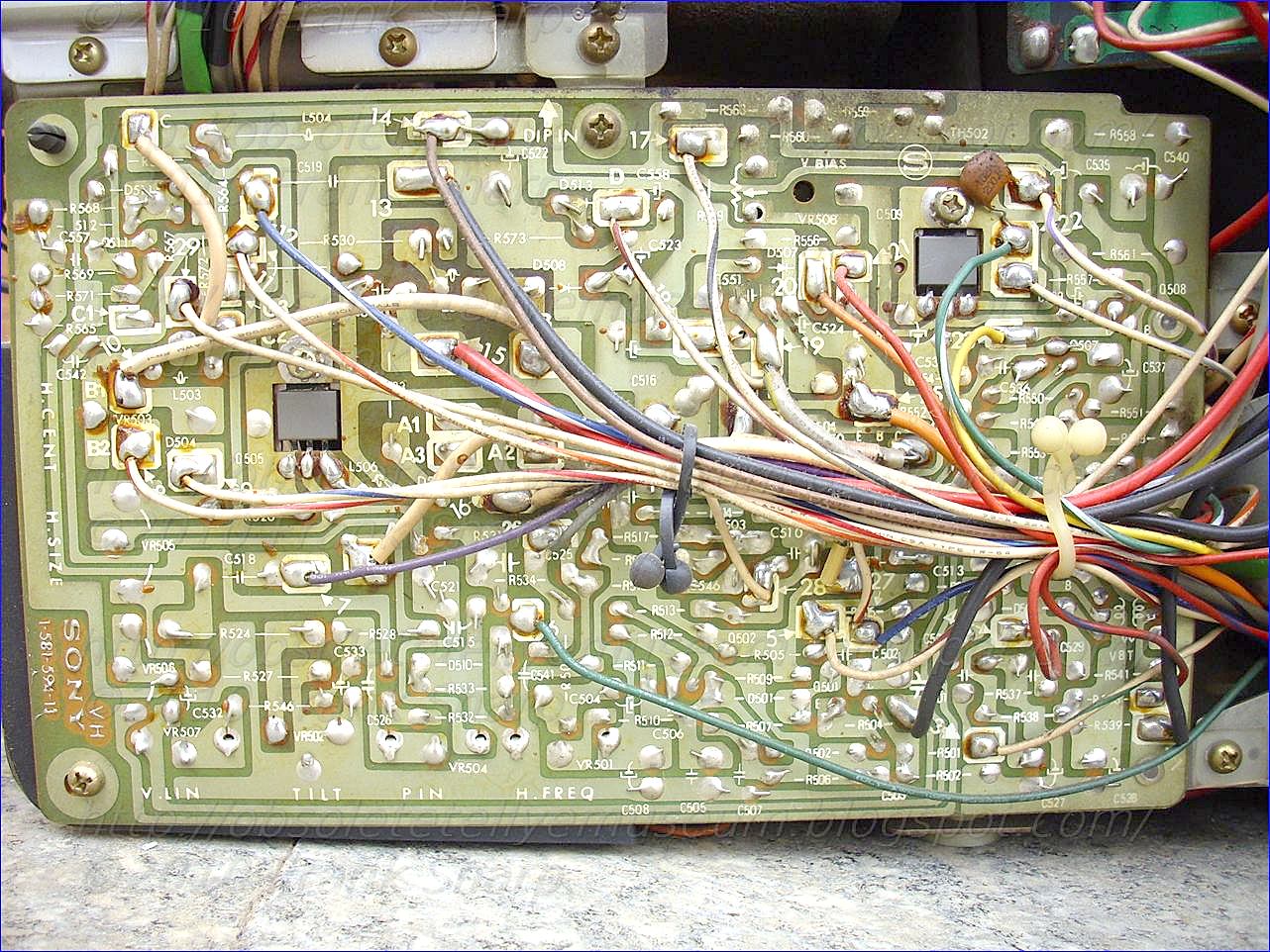


The CHASSIS of the SONY KV-1300E is a good example of Japanese Electronics Engineering.
Chassis technology is entirely based on semiconductors.
On left side is located the SMPS Power supply and the tuning selectors.
On bottom side at floor level All signal processing stages inclusive Luminance and chrominance.
The signal processing at IF level is demande to the middle left vertical board.
Right side All deflection and EHT stages inclusive all classic corrections needed by a SONY Trintron system.
Power supply and line deflection are realized with special Thyristor technology called Silicon-Controlled Switch (SCS)he silicon controlled switch (SCS) is the next step beyond the silicon controlled rectifier (SCR). It is still a four-layer diode, but this time all four regions are accessible to the external circuit.
The basic construction of the SCS is the same as for the SCR, with the addition of a second gate lead. We thus have an anode, a cathode, an anode gate, and a cathode gate. The equivalent circuit is the same as shown to the right, and even the schematic symbol of the SCS is similar to the SCR symbol.
The SCS has two advantages over the SCR and the four-layer diode. First, because both gate regions are accessible, they can be biased so as to completely cancel the rate effect we described with the four-layer diode. Second, since we can now control both end junctions, we can actively turn the SCS off without having to reduce the applied voltage or current. Thus, the SCS really is a switch, and can be used as one.HORIZONTAL DEFLECTION CIRCUIT SONY KV-1300E :
A solid-state horizontal deflection circuit including a high voltage applying circuit for a television receiver or the like in which a gate-controlled switching device is used for applying a deflection current to a horizontal deflection coil to perform horizontal beam scanning and another semiconductor switching device is used for applying a pulse voltage to a flyback transformer to produce a high voltage supplied to a cathode ray tube, and further a couple of diodes connected in series are provided in connection with the above two switching devices. Both switching devices are turned on in response to a horizontal driving signal supplied to at least one of them and turned off by the recovery current of the series-connected diodes.
What is claimed is
1. A horizontal deflection circuit including a high voltage producing circuit comprising:
2. A horizontal deflection circuit according to claim 1, in which the third electrode of said gate-controlled switching device is directly grounded.
3. A horizontal deflection circuit according to claim 1, comprising, in addition, a resistor, one end of said series connection of the diodes being connected to the third electrode of said semiconductor switching device and the other end being grounded through a resistor.
4. A horizontal deflection circuit according to claim 3, in which said coupling means comprises a capacitor and a resistor connected in parallel to each other.
5. A horizontal deflection circuit according to claim 4, in which said semiconductor switching device comprises a second gate-controlled switching device, the gate of said second gate-controlled switching device being connected to said driving signal source.
6. A horizontal deflection circuit according to claim 3, in which said semiconductor switching device comprises a transistor, the base and emitter electrodes of said transistor being connected to said driving signal source.
7. A horizontal deflection circuit according to claim 1, in which said coupling means comprises an additional signal source.
8. A horizontal deflection circuit according to claim 7, in which said coupling means further comprises a parallel connection of a capacitor and a resistor coupled in series with said additional signal source.
9. A horizontal deflection circuit according to claim 8, in which said driving signal source and additional signal source comprise a driving transformer having a plurality of windings.
10. A horizontal deflection circuit according to claim 9, in which said semiconductor switching device comprises another gate-controlled switching device.
11. A horizontal deflection circuit according to claim 9, in which said semiconductor switching device comprises a transistor having an additional current path provided between the base and emitter electrodes thereof.
Description:
BACKGROUND OF THE INVENTION
1. Field of the Invention
This invention relates generally to horizontal deflection circuits for a television receiver or the like and more particularly to a solid-state horizontal deflection circuit including a high voltage producing circuit and using a gate-controlled switching device for applying a deflection current to a horizontal deflection coil.
2. Description of the Prior Art
In solid-state horizontal deflection circuits for use in television receivers or the like, a switching element employed in the horizontal output stage is required to withstand a high voltage and must be capable of carrying large current. It is the practice in the art to employ a specially selected, expensive transistor of large current carrying capacity and high inverse voltage. In order to avoid the use of such an expensive transistor, a proposal has been made to employ a cheaper thyristor, for example, a semiconductor device referred to as a gate-controlled switch (GCS). This GCS is sometimes called a GTO (a gate turnoff switch). The GCS consists of a first P-type semiconductor layer, a first N-type semiconductor layer, a second P-type semiconductor layer and a second N-type semiconductor layer. The first P-type layer serves as an anode; the second N-type layer, a cathode; and the second P-type layer, a gate. A gate current is applied between the gate and cathode to control the conductivity between the anode and cathode. Once the switch has been turned on or off by the gate current between the gate and cathode, it remains in the on or off state even without continuing to apply the gate current to it, so that it is capable of being switched by a low power source and is suitable for use as a switching element of the horizontal deflection circuit. Further, generally, a horizontal deflection pulse produced by the operation of the switching element of the horizontal deflection circuit is boosted by a flyback transformer and rectified to serve as the high voltage for the cathode ray picture tube. However, prior horizontal deflection circuits using such a thyristor have defects such as complexity in the construction for operating the thyristor, deterioration of the horizontal deflection current, and so on.
It is one object of this invention to provide an improved solid-state horizontal deflection circuit using a gate-controlled switching device.
Another object of this invention is to provide a horizontal deflection circuit using a gate-controlled switching device effectively controlled by an improved gate current applying system.
A further object of this invention is to provide a horizontal deflection circuit using a gate-controlled switching device and producing a horizontal deflection current of high quality.
Still a further object of this invention is to provide a solid-state horizontal deflection circuit including a high voltage producing circuit in which a gate-controlled switching device and another semiconductor switching device are provided for producing, respectively, a horizontal deflection current and a pulse voltage to make a high voltage applied to a cathode ray tube and both switching devices are coupled with each other to operate with improved efficiency.
Other objects and aspects of this invention will be apparent from the following specification, together with drawings.
SUMMARY OF THE INVENTION
This invention is directed to a horizontal deflection circuit employing such a GCS as abovementioned in which a switching element for supplying a horizontal deflection current to a deflection coil and a switching element for generating a pulse voltage necessary for producing a high voltage to be supplied to a cathode ray tube are separately provided and at least the former switching element is a GCS.
BRIEF DESCRIPTION OF THE DRAWINGS
FIG. 1 is a connection diagram showing one example of a horizontal deflection circuit of this invention;
FIGS. 2A-2I are a series of waveform diagrams for explaining the operation of the circuit exemplified in FIG. 1;
FIGS. 3 and 4 are connection diagrams illustrating modified forms of the horizontal deflection circuit of this invention;

FIGS. 5A-5H are a series of waveform diagrams for explaining the operation of the circuit depicted in FIG. 4; and
FIG. 6 is a connection diagram showing another modified form of the horizontal deflection circuit of this invention.
DESCRIPTION OF THE PREFERRED EMBODIMENTS
With reference to FIG. 1 a horizontal deflection circuit of this invention with hereinafter be described in detail. A driving transistor 1 is supplied with a rectangular wave signal produced by a horizontal oscillating circuit, which may be of standard construction and is, therefore, not shown, synchronized wiJh a horizontal synchronizing signal. Reference numeral 2 designates a transformer having a primary winding 3a, a secondary winding 3b, and a tertiary winding 3c. A high voltage generating circuit 4 is connectdd to the transformer 2 and comprises a fly-back transformer 5 that has primary and secondary windings 6a and 6b. A switching element 7, which, in the present example, is a GCS, is connected to the primary 6a. A damper diode 8 and a capacitor 9 are also connected to the primary 6a. A rectifier 10 connects the secondary 6b to a cathode ray tube 11. The secondary winding 3b of the driving transformer 2 is grounded through a parallel circuit 25 consisting of a capacitor 24 and a resistor 23. Reference numeral 12 indicates generally a horizontal deflection current generating circuit that includes a horizontal deflection transformer or choke 13, a horizontal deflection coil 14, and a capacitor 15 connected in series thereto. A damper diode 16, a capacitor 17, and a GCS 18 are connected in parallel with the series connected coil 14 and capacitor 15. A direct voltage source 19 furnishes power for the circuit 4, and a second source 20 furnishes power for the circuit 12.
In the present invention, first and second diodes 21 and 22 are connected in the same polarity as the GCS 7 between the cathode of the switching element (the GCS 7 in the example of FIG. 1) and ground. The secondary winding 3b of the transformer 2 is connected at one end to the gate of the GCS 7 and grounded at the other end through the parallel circuit 25. The tertiary winding 3c is connected at one end to the connection point of the diodes 21 and 22 through a parallel circuit 28 consisting of a resistor 26 and a capacitor 27 and is connected at the other end to the gate of the GCS 18. The secondary and tertiary windings 3b and 3c of the transformer 2 are adapted to derive signals of opposite polarities, and in the drawings black dots indicate those ends of the primary, secondary, and tertiary windings 3a, 3b and 3c of the transformer 2 which are the same in polarity.
With such an arrangement, when a rectangular wave voltage S 1 , such as is shown in FIG. 2A, is applied through the transistor 1 to the primary winding 3a of the transformer 2, rectangular wave voltages S 2 and S 3 , such as are depicted in FIGS. 2B and 2C, are derived at the
 secondary and tertiary windings 3b and 3c. Accordingly, when the voltage S 2 rises at a time t 1 , a gate current i 0 of the GCS's 7 and 18, such as shown in FIG. 2D, flows in a circuit along the path P 0 to turn on the GCS's 7 and 18. The anode currents I 1 and I 2 (currents flowing between the anodes and cathodes) of the GCS's 7 and 18, shown in FIGS. 2E and 2F, flow therethrough from the time t 1 to t 2 (the positive half cycle of the voltage S 2 ). The waveform of the current I 2 is identical with that of a current flowing in the horizontal deflection coil 14 of the horizontal deflection current generating circuit 12. In this case, at the rising of the rectangular wave voltage S 2 , the gate current i 0 is about to flow through the diode 22, but the voltage S 3 induced in the tertiary coil 3c is opposite in sense to that S 2 in the secondary coil 3b and is impressed through the gate and cathode of the GCS 18 to the diode 22 to put it in reverse biased condition and hence hold the diode 22 nonconductive. Accordingly, the aforementioned gate current i 0 does not flow to the diode 22 and the voltage S 2 induced in the winding 3b biases the GCS in the forward direction between its gate and cathode to put it in the "on" state. The voltages S 3 and S 2 induced in the windings 3c and 3b are superimposed on each other to bias the GCS 18 in the forward direction between its gate and cathode to cause it to conduct. As the gate current i 0 and the anode current I 1 of the GCS 7 flows in the aforementioned path and charges the capacitor 27, the anode potential of the diode 22 gradually rises to bias the diode 22 in the forward direction to cause it to conduct. Therefore, one portion of the gate current i 0 and almost all of the gate current I 1 of the GCS 7, which gradually increases because of its being a sawtooth wave, flow in the diode 22. The diode 22 plays an important role to provide a path which prevents the anode current of the GCS 7 from flowing in the GCS 18 except at its rising.
When the rectangular wave voltage S 1 falls at the time t 2 , the aforementioned voltage S 2 also falls and a gate current i 0 ' flows in a path opposite in direction to the path P 0 of the gate current i 0 . The current i 0 ' flows for a period of time during which the so-called recovery currents of the diodes 21 and 22 flow. The GCS's 7 and 18 are thereby turned off to stop the flow of the anode currents I 1 and I 2 of the GCS's 7 and 18. In this case, the value E c of the voltage S 3 produced across the tertiary winding 3c is selected to be smaller than the value V 1 of the breakdown voltage between the gate and cathode of the GCS 18. Mathematically, E c < V 1 . The sum of the value E b of the voltage S 2 produced across the secondary winding 3b and the aforementioned voltage value E c is selected to be greater than the sum of the value V 2 of the breakdown voltage between the gate and cathode of the GCS 7 and the aforementioned voltage value V 1 . That is, E b + E c > V 1 + V 2 . Under such conditions the gate current is applied to the GCS's 7 and 18 for the time of circulation of the aforementioned recovery current. Moreover, the diodes 21 and 22 are put in the reverse biased condition at the time t 2 when the rectangular wave voltage S 2 falls and the recovery current of the diodes 21 and 22 flows, as the gate current i 0 ' for the GCS 7, from the diode 22 to the resistor 23 through the diode 21, the cathode and gate of the GCS 7 and the secondary winding 3b of the transformer 2, by which the GCS 7 is turned off substantially at the time t 2 . At that time, no current flows from the cathode of the GCS 18 to the diode 21 through the gate of the GCS 18, the winding 3c and the resistor 26 due to the aforementioned relationship E c < V 1 .
 However, the forward current flowing in the diode 22 when the GCS's 7 and 18 are in the "on" state is less than the forward current flowing in the diode 22, so that the time during which the recovery current of the diode 22 flows is shorter than that during which the recovery current of the diode 21 flows. Therefore, the reverse current flowing in the diode 22 stops at the time t 3 , after which the recovery current of the diode 21 flows as a gate current i 0 ", shown in FIG. 2G, through the path P 0 of the current i 0 , by which the GCS 18 is turned off substantially at the time t 2 due to the aforementioned relationship E b + E c > V 1 + V 2 . The recovery current of the diode 21 stops at the time t 4 .
After a time t 5 , a current I 3 , such as depicted in FIG. 2H, flows in the deflection coil 14 through the damper diode 16 and at a time t 6 the voltage S 1 rises again. Thereafter the same operations as above described are repeatedly carried out to supply the deflection coil 14 with a current I 4 , shown in FIG. 21. Further, the primary winding 6a of the flyback transformer 5 of the high voltage producing circuit 4 is supplied with a pulse voltage by the on-off operation of the GCS 7, so that the pulse is boosted by the secondary winding 6b and is rectified by the diode 10 to provide a high voltage, which is supplied to the anode of the cathode ray tube 11.
FIG. 3 illustrates another embodiment of this invention in which elements similar to those in FIG. 1 are marked with the same reference numerals and in which the GCS 7 of the high voltage producing circuit 4 is replaced with a transistor 31. The transistor 31 is turned on and off by the rectangular wave voltage S 2 induced in the secondary winding 3b of the drive transformer 2, but the GCS 18 is turned off by the recovery current of the diode 21 as is the case in FIG. 1. The other operations are the same as those in the example of FIG. 1, and, accordingly, no detailed description will be repeated. Reference numeral 29 indicates a diode connected between the base and emitter of the transistor 31, which is provided for preventing breakdown of the transistor 31 when its recovery current flows, but this diode is not always necessary.
In the present invention, since the output currents from the secondary and tertiary windings 3b and 3c of the transformer 2 are superimposed on each other and applied to the control electrodes of the switching element 7 and the GCS 18, that is, to the gate current path as above described, the GCS's 18 and 7 can be turned on and off without fail. In the illustrated example, the parallel circuit 28 is interposed between the connection point of the diodes 21 and 22 and the tertiary winding 3c but may be connected between the gate of the GCS 18 and the tertiary winding 3c.
In the example of FIG. 1, the connection point of the horizontal deflection coil 14 and the capacitor 15 is connected through the capacitor 30 to the connection point of the secondary winding 3b and the parallel circuit 25. With such a connection, a parabolic voltage generated at the connection point of the horizontal deflection coil 14 and the capacitor 15 is applied to the connection point of the secondary winding 3b and the parallel circuit 25, thereby to facilitate turning on and off the GCS 7. Due to this parabolic voltage, the gate potential of the GCS 7 is raised at the time of turning on the GCS 7 and lowered at the time of turning it off.
FIG. 4 illustrates another embodiment of this invention in which the tertiary winding 3c of the drive transformer 2 in the example of FIG. 2 is not employed and the connection point of the diodes 21 and 22 is connected directly to the gate of the GCS 18 through the parallel circuit 28 of the resistor 26 and the capacitor 27. Further, the cathode of the diode 22 is grounded through a resistor 32. The on-off and other operations of the GCS's 7 and 18 are also substantially the same in this embodiment as in the embodiment of FIG. 2. However, the present example is different from that of FIG. 2 in that the gate current of the GCS's 7 and 18 and the anode current of the GCS 7, having passed through the diode 21, are shunted from a path leading to the diode 22 and the resistor 32 to a path leading to the gate of the GCS 18 through the parallel circuit of the resistor 26 and the capacitor 26. The resistor 32 is provided to direct the shunted current to the gate of the GCS 18 and its resistance value is selected to permit flowing of the shunted current as a gate current enough to turn on the GCS 18.
A detailed description will be given of the circuit in FIG. 4. A rectangular wave voltage S 1 , such as shown in FIG. 5A, is supplied to the primary winding 3a of the drive transformer 2 so that a rectangular wave voltage S 2 , such as depicted in FIG. 5B, is induced in the secondary winding 3b. From the time t 1 of rising of the rectangular wave voltage S 2 , a gate current i 1 to the GCS 7, such as shown in FIG. 5C, flows in a path from the secondary winding 3b through the gate of the GCS 7, its cathode, the diode 21, the diode 22, the resistor 32, and the parallel circuit 25 of the resistor 23 and the capacitor 24 back to the secondary winding 3b. Further, the gate current i 1 is also shunted to the gate and cathode of the GCS 18. As a result, the GCS 7 is turned on at the time t 1 . When the GCS 7 is turned on, an anode current I 1 of the GCS 7 as depicted in FIG. 5D is shunted to the diodes 21 and 22 from the GCS 7 and to the gate and cathode of the GCS 18 through the parallel circuit 28 of the resistor 26 and the capacitor 27 from the GCS 7. Consequently, a gate current i 2 , such as depicted in FIG. 5E, that consists of one portion of the gate current i 1 and one portion of the anode current I 1 of the GCS 18 superimposed upon each other, flows in the gate and cathode of the GCS 18 to turn it on at the time t 1 . This causes an anode current I 2 , such as shown in FIG. 5F, to flow in the GCS 18. The anode current I 2 is supplied to the deflection coil 14. In this case, the value of the gate current i 2 of the GCS 18 is suitably selected dependent upon the values of the resistors 32 and 26. Further, the gate current i 2 is controlled by the capacitor 27 so that it does not increase excessively relative to the increase in the anode current I 1 of the GCS 7.
At the time t 2 when the rectangular wave voltage S 1 falls, the rectangular wave voltage S 2 becomes negative and the gate current i 1 is stopped and, at the same time, the diodes 21 and 22 are put in reverse biased condition, so that the recovery current of the diodes 21 and 22 flow as a gate current i 1 ' of the GCS 7 through the resistor 32, the diodes 22 and 21, the cathode and gate of the GCS 7, the secondary winding 3b and the parallel circuit 25 of the resistor 23 and the capacitor 24, thereby turning off the GCS 7. Therefore, the anode current I 1 of the GCS 7 stops substantially at the time t 2 . In this case, the forward current flowing in the diode 22 from the time t 1 to t 2 is less than the forward current flowing in the diode 21 by the amount corresponding to the gate current i 2 of the GCS 18. Consequently, the time during which the recovery current of the diode 22 flows is shorter than that of the diode 21. Accordingly, while the recovery current of the diode 21 is still flowing, that of the diode 22 stops flowing at a time t 3 and the recovery current of the diode 21 flows as a gate current i 2 ' of the GCS 18 through the cathode and gate of the GCS 18, the parallel circuit 28 of the resistor 26 and the capacitor 27, the diode 21 and the GCS 7, causing the GCS 18 to be turned off. Consequently, the anode current I 2 of the GCS 18 stops flowing substantially at the time t 3 . The flow of the recovery current of the diode 21 stops at a time t 4 . Thereafter, a damper current I 3 , such as depicted in FIG. 5G, flows from a time t 5 , so that the deflection coil 14 is supplied with a horizontal deflection current I, such as shown in FIG. 5H. Further, the primary winding of the flyback transformer 5 is supplied with a pulse of a predetermined width which is generated when the anode current I 1 of the GCS 7 stops. The pulse is derived from the secondary winding of the flyback transformer 5 after being boosted and then it is rectified to provide a high voltage. Thereafter, the rectangular wave voltage S 1 rises again at a time t 6 and the foregoing operations are repeated.
FIG. 6 shows another example of this invention which employs the transistor 31 in place of the GCS 7 of FIG. 4, as is the case with FIG. 3, and which is the same in operation as the example of FIG. 3. Therefore, no detailed description will be given, but, in this case, the recovery currents of the diodes 21 and 22 do not flow in the transistor 34 through the short path 33.
As has been described in the foregoing, in the present invention a series circuit of two diodes is connected to the cathode of, for example, a GCS serving as a first switching device of a high voltage generating circuit and a GCS serving as a second switching device of a horizontal deflection current applying circuit is connected to the series circuit and the switching of both of the switching devices is controlled by a voltage derived from the secondary winding of a drive transformer. In this invention, the series circuit is provided for coupling the switching devices in the current path of the secondary winding of the drive transformer, so that the circuit construction is simple as a whole. Further, since the two switching devices, at least one of which is a GCS, are controlled only by the voltage induced in the secondary winding, the horizontal deflection circuit of this invention is low in power dissipation and hence is economical.
Moreover, no nonlinear characteristic element such as a transistor, diode or the like is inserted in the anode current path of the GCS acting as a switching device used in the horizontal deflection current applying circuit. Therefore, the linearity of the horizontal deflection current flowing in the deflection coil is never impaired and a horizontal deflection current of high quality can be obtained.
It will be apparent that many modifications and variations may be effected without departing from the scope of the novel concepts of this invention.
The interesting part , toghether with the rest, is the uncommon plug to "Inject" the Focusing voltage direcltly in the CRT TUBE NECK ! ! ! ! !
CONVERGENCE DEFLECTION SYSTEM FOR A SONY TRINTRON COLOR PICTURE TUBE
In a color picture tube in which a plurality of beams are made to intersect each other at a location between the beam generating sources and the color screen and are focused on the latter by a main focusing lens positioned to dispose its optical center substantially at the location where the beams intersect so that beams emerge from such lens along divergent paths, first and second spaced plates are disposed at opposite sides of each of the divergent paths to electrostatically deflect the respective beam and cause convergence of all of the beams at a common area on the screen when the first and second plates are at different potentials, a high voltage is generated from a horizontal deflecting pulse provided for causing the beams to scan the screen and such high voltage is applied to an anode electrode of the tube and also to each first plate, and a static convergence deflecting voltage is obtained by dividing the aforementioned high voltage and is applied as the potential difference between the first and second plates by which the respective beam is to be deflected. Further, a dynamic convergence deflecting voltage, comprising both parabolic and sawtooth voltages is generated in response to the horizontal deflecting pulse and is superimposed on the static convergence deflecting voltage with provision being made for separately adjusting both deflecting voltages.
1. In a single-gun, plural-beam cathode-ray tube which includes a beam-receiving screen, beam-generating means for directing a plurality of electron beams toward said screen, and lens means for focusing said electron beams on said screen and having an optical center through which said beams are all passed with at least two of said beams emerging from said lens means along paths which are divergent to the optical axis of the latter; electron beam convergence-deflecting means to deflect said beams emerging along said divergent paths for convergence of said beams at a common area of said screen, said convergence-deflecting means comprising first and second spaced plates disposed at opposite sides of each of said divergent paths for electrostatically deflecting the respective beam when at different electrical potentials, high voltage-generating means receiving a horizontal deflecting pulse and operative to generate a high voltage therefrom, means to apply said high voltage as an anode voltage in said tube and also to said first plate associated with each divergent path, voltage-dividing means dividing said high voltage to produce a static convergence deflecting voltage, and means to apply said static convergence voltage between said first plate and said second plate associated with each divergent path and thereby establish the potential difference therebetween for deflecting the respective beam.
2. A single-gun, plural-beam cathode-ray tube according to claim 1, in which said voltage-dividing means includes first and second series connected resistors having said high voltage applied thereacross so that said static convergence-deflecting voltage appears across one of said resistors.
3. A single-gun, plural-beam cathode-ray tube according to claim 2, in which one of said resistors is variable to permit adjustment of said static convergence-deflecting voltage obtained by dividing said high voltage.
4. A single-gun, plural-beam cathode-ray ray tube according to claim 2, in which capacitors are respectively connected in parallel with said first and second resistors for stabilizing the voltages appearing thereacross.
5. A single-gun, plural-beam cathode-ray tube according to claim 2, in which there are provided means to generate a dynamic convergence-deflecting voltage, and means to superimpose said dynamic convergence voltage on said static convergence voltage.
6. A single-gun, plural-beam cathode-ray tube according to claim 5, in which said means to superimpose the dynamic convergence voltage on the static convergence voltage is an isolating transformer connected to said means to generate the dynamic convergence-deflecting voltage and to said voltage-dividing means.
7. A single-gun, plural-beam cathode-ray tube according to claim 6, in which said isolating transformer has a primary winding connected with said means to generate the dynamic convergence-deflecting voltage and a secondary winding connected in series between said first and second resistors of said voltage dividing means.
8. A single-gun, plural-beam cathode-ray tube according to claim 6, in which said isolating transformer has a primary winding connected with said means to generate the dynamic convergence-deflecting voltage and a secondary winding connected at one end to a connecting point between said first and second resistors of said voltage-dividing means and at the other end to said second plate associated with each of said divergent paths.
9. A single-gun, plural-beam cathode-ray tube according to claim 5, in which the tube has a horizontal deflection coil to cause the beams to horizontally scan the screen when a horizontal deflecting current of sawtooth configuration flows through said coil, and in which said means to generate a dynamic convergence-deflecting voltage includes means to derive from said horizontal deflecting current flowing through said coil a voltage of parabolic waveform, means operating in synchronism with said horizontal deflecting current to produce a voltage of sawtooth waveform and means to combine the voltages of parabolic and sawtooth waveform for constituting said dynamic convergence deflecting voltage.
10. A single-gun, plural-beam cathode-ray tube according to claim 9, in which means are provided to separately adjust the magnitude of said voltage of parabolic waveform and the magnitude and wave shape of said voltage of sawtooth waveform.
11. A single-gun, plural-beam cathode-ray tube according to claim 9, in which a capacitor is connected in series with said horizontal deflection coil to produce a voltage of parabolic waveform across said capacitor, capacitive means divides said voltage across said capacitor to provide said voltage of parabolic waveform to be combined with said voltage of sawtooth waveform, and variable inductor means is connected between said capacitance means and said means to superimpose the dynamic convergence voltage on the static convergence voltage to adjust the magnitude of said voltage of parabolic waveform thus combined.
12. A single-gun, plural-beam cathode-ray tube according to claim 11, in which said means to produce the voltage of sawtooth waveform includes a flyback transformer driven in synchronism with said horizontal deflection current and having a secondary winding, a potentiometer having a resistance and a slider movable therealong, and an inductor connected in series with said potentiometer resistance across said secondary winding to produce a voltage of sawtooth configuration across said resistance, with said voltage of sawtooth waveform to be combined with said voltage of parabolic waveform appearing at said slider of the potentiometer.
13. A single-gun, plural-beam cathode-ray tube according to claim 12, in which said means to superimpose said dynamic and static convergence voltages includes an isolating transformer having a primary winding connected to said slider of the potentiometer and to said variable inductor means.
14. Horizontal dynamic convergence voltage-generating means for a cathode-ray tube having a horizontal deflection coil to effect horizontal beam scanning in response to the passage therethrough of a horizontal deflecting current of sawtooth configuration, comprising means operating in synchronism with said horizontal deflecting current to produce a voltage of sawtooth waveform, a capacitor connected in series with said horizontal deflection coil to produce a first voltage of parabolic waveform across said capacitor, capacitive means dividing said first voltage across said capacitor to provide a second voltage of parabolic waveform, means to combine said second voltage of parabolic waveform with said voltage of sawtooth waveform, and variable inductor means connected between said capacitance means and said means to combine said second voltage of parabolic waveform with said voltage of sawtooth waveform to adjust the magnitude of said second voltage of parabolic waveform thus combined.
15. Horizontal dynamic convergence voltage-generating means according to claim 14, in which said means to produce the voltage of sawtooth waveform includes a flyback transformer driven in synchronism with said horizontal deflection current and having a secondary winding, a potentiometer having a resistance and a slider movable therealong, and an inductor connected in series with said potentiometer resistance across said secondary winding to produce a voltage of sawtooth configuration across said resistance, with said voltage of sawtooth waveform to be combined with said voltage of parabolic waveform appearing at said slider of the potentiometer.
16. Horizontal dynamic convergence voltage-generating means according to claim 15, in combination with means to produce a static convergence-deflecting voltage, and means to superimpose said dynamic convergence-deflecting voltage on said static convergence-deflecting voltage including isolating transformer means having a primary winding connected, at its ends, to said variable inductor means and to said slider, respectively.
Description:


This invention relates generally to color picture tubes of the single-gun, plural-beam type, and particularly to tubes of that type in which the plural beams are passed through the optical center of a common electron lens by which the beams are focused on the color phosphor screen.
In single-gun, plural-beam color picture tubes of the described type, for example, as specifically disclosed in the U.S. Pat. No. 3,448,316, issued June 3, 1969 and having a common assignee herewith, three electron beams are emitted or originated by a beam generating or cathode assembly so that one central beam coincides with the optical axis of the electron focusing lens and the two other beams are converged to cross the central beam substantially at the optical center of the lens and thus emerge from the latter along paths that are divergent from the optical axis. Arranged along opposite sides of each of such divergent paths are first and second convergence-deflecting plates at different electrical potentials to deflect the respective beam for causing all beams to converge at a point on the aperture grill or other beam selecting means associated with the color screen, and from which the beams again diverge to impinge on respective phosphor stripes or dots of the screen. After passing between the convergence-deflecting plates, the beams are acted upon by the magnetic fields resulting from the application of horizontal and vertical sweep signals to the corresponding coils of a deflection yoke, whereby the beams are made to scan the screen in the desired raster. It will be apparent that the accurate convergence of the beams at the aperture grill or other beam-selecting means of the tube is dependent upon the convergence-deflecting voltages applied between the plates.
Accordingly, it is an object of this invention to provide a color picture tube of the described type with an improved circuit arrangement by which the convergence-deflecting voltages are generated.
Another object is to provide a circuit arrangement, as above, which produces a static convergence voltage from a high voltage applied to the tube anode, and wherein variations in the anode voltage are accurately reflected in corresponding charges in the static convergence voltage so as to maintain the proper convergence of the beams.
Another object is to provide a circuit arrangement, as above, which produces a horizontal dynamic convergence voltage superimposed on the static convergence voltage while isolating the source of such dynamic convergence voltage from the static convergence voltage.
Still another object is to provide a circuit arrangement, as above, and in which the static and dynamic convergence voltages can be individually controlled without danger from high voltages.
A further object is to provide a circuit arrangement, as above, with improved means for producing the dynamic convergence voltage.
In accordance with an aspect of this invention, the high voltage applied to an anode electrode of the color picture tube and to one of the convergence deflecting plates associated with each divergent path is generated from a horizontal deflecting pulse provided for causing horizontal scanning of the beams, and the static convergence-deflecting voltage applied between the convergence-deflecting plates associated with each divergent path is obtained by dividing the mentioned high voltage.
Further, in accordance with the invention, the dynamic convergence-deflecting voltage which is superimposed on the static convergence-deflecting voltage is generated in response to the horizontal deflecting pulse.
The above, and other objects, features and advantages of the invention, will be apparent in the following detailed description of illustrative embodiments thereof which is to be read in connection with the accompanying drawings, wherein:
FIG. 1 is a schematic sectional view in a horizontal plane passing through the axis of a single-gun, plural-beam color picture tube and which is shown provided with a convergence deflection system according to one embodiment of this invention;
FIGS. 2A-2E are graphic representations of the wave forms of the static and dynamic convergence deflection voltages produced according to this invention; and
FIG. 3 is a diagrammatic view showing a modification of the convergence deflection system of FIG. 1.
Referring now to the drawings in detail, and initially to FIG. 1 thereof, it will be seen that a single-gun, plural-beam color picture tube of the type to which this invention is applied may comprise a glass envelope (not shown) having a neck and a cone extending from the neck to a color Screen S provided with the usual arrays of color phosphors S R , S G and S B and with an aperture grill G P or beam-selecting means, such as a so-called shadow mask. Disposed within the neck is a single electron gun A having cathodes K R , K G and K B , each of which is constituted by a beam-generating source with the respective beam-generating surfaces thereof disposed as shown in a plane which is substantially perpendicular to the axis of the electron gun. In the embodiment shown, the beam-generating surfaces thereof are arranged in a straight line so that the respective beams B R , B G and B B emitted therefrom are directed in a substantially horizontal plane containing the axis of the gun, with the central beam B G being coincident with such axis. A first grid G 1 is spaced from the beam-generating surfaces of cathodes K R , K G and K B and has apertures g 1R , g 1G and g 1B formed therein in alignment with the respective cathode beam-generating surfaces. A common grid G 2 is spaced from the first grid G 1 and has apertures g 2R , g 2G and g 2B formed therein in alignment with the respective apertures of the first grid G 1 . Successively arranged in the axial direction away from the common grid G 2 are open-ended, tubular grids or electrodes G 3 , G 4 and G 5 , respectively, with cathodes K R , K G and K B , grids G 1 and G 2 , and electrodes G 3 , G 4 and G 5 being maintained in the depicted assembled positions thereof, by suitable, nonillustrated support means of an insulating material.
For operation of the electron gun of FIG. 1, appropriate voltages are applied to the grids G 1 and G 2 and to the electrodes G 3 , G 4 and G 5 . Thus, for example, a voltage of 0 to minus 400 v. is applied to the grid G 1 , a voltage of 0 to 500 v. is applied to the grid G 2 , a voltage of 13 to 20 kv. is applied to the electrodes G 3 and G 5 , and a voltage of 0 to 400v. is applied to the electrode G 4 , with all of these voltages being based upon the cathode voltage as a reference. As a result, the voltage distributions between the respective electrodes and cathodes, and the respective lengths and diameters thereof, may be substantially identical with those of a unipotential single beam-type electron gun which is constituted by a single cathode and first and second, single-apertured grids.
With the applied voltage distribution as described hereinabove, an electron lens field will be established between grid G 2 and the electrode G 3 to form an auxiliary lens L' as indicated in dashed line, and an electron lens field will be established around the axis of the electrode G 4 , by the electrodes G 3 , G 4 and G 5 , to form a main lens L, again as indicated in dashed lines.
Further included in the electron gun of FIG. 1 are electron beam convergence deflecting means F which comprise shielding plates P and P' disposed in the depicted spaced, relationship at opposite sides of the gun axis, and axially extending, deflector plates Q and Q' which are disposed, as shown, in outwardly spaced, opposed relationship to shielding plates P and P', respectively. Although depicted as substantially straight, it is to be understood that the deflector plates Q and Q' may, alternatively, be somewhat curved or outwardly bowed, as is well known in the art.
The shielding plates P and P' are equally charged and disposed so that the central electron beam B G will pass substantially undeflected between the shielding plates P and P', while the deflector plates Q and Q' have negative charges with respect to the plates P and P' so that respective electron beams B B and B R will be convergently deflected as shown by the respective passages thereof between the plates P and Q and the plates P' and Q'. More specifically, a voltage V P which is equal to the voltage applied to the electrodes G 3 and G 5 , may be applied to both shielding plates P and P', and a voltage V Q , which is some 200 to 300 v. lower than the voltage V P , is applied to the respective deflector plates Q and Q' to result in the respective shielding plates P and P' being at the same potential, and to result in the application of a deflecting voltage difference or static convergence deflecting voltages V C between the respective plates P' and Q' and P and Q and it is, of course, this convergence-deflecting voltage V C which will impart the requisite convergent deflection to the respective electron beams B B and B R .
In operation, the respective electron beams B R , B G and B B which emanate from the beam-generating surfaces of the cathodes K R , K G and K B will pass through the respective grid apertures g 1R , g 1G and g 1B , to be intensity modulated with what may be termed the "red", "green" and "blue" intensity modulation signals applied between the said cathodes and the first grid G 1 . The respective electron beams will then pass through the common auxiliary lens L' to cross each other substantially at the optical center of the main lens L and to emerge from the latter with beams B R and B B diverging from beam B G . Thereafter, the central electron beam B G will pass substantially undeflected between shielding plates P and P' since the latter are at the same potential. Passage of the electron beam B B between the plates P' and Q' and of the electron beam B R between the plates P and Q will, however, result in the convergent deflections thereof as a result of the convergence-deflecting voltage applied therebetween, and the system of FIG. 1 is so arranged that the electron beams B B , B G and B R will desirably converge or cross each other at a common spot centered in an aperture of the aperture grill G P or other beam selecting means so as to diverge therefrom to strike the respective color phosphors of a corresponding array thereof on screen S. More specifically, it may be noted that the color phosphor screen S is composed of a large plurality of sets or arrays of vertically extending "red", "green" and "blue" phosphor stripes or dots S R , S G and S B with each of the arrays or sets of color phosphors forming a color picture element. Thus, it will be understood that the common spot of beam convergence corresponds to one of the thusly formed color picture elements.
The voltage V P applied to the lens electrodes G 3 and G 5 and to plates P and P', is also applied to the screen S as an anode voltage in conventional manner through a nonillustrated graphite layer which is provided on the inner surface of the cone of the tube envelope. Thus, to summarize the operation of the depicted color picture tube of FIG. 1, the respective electron beams B B , B G and B R will be converged at aperture grill G P and will diverge therefrom in such manner that electron beam B B will strike the "blue" phosphor S B , electron beam B G will strike the "green" phosphor S G and electron beam B R will strike the "red" phosphor S R of the array or set corresponding to the aperture at which the beams converge. Electron beam scanning of the face of the color phosphor screen is effected by horizontal and vertical deflection yoke means which receives horizontal and vertical sweep signals whereby a color picture will be provided on the color screen. Since, with this arrangement, the respective electron beams are each passed, for focusing, through the center of the main lens L of the electron gun A, the beam spot formed by impingement of the beams on the color phosphor screen S will be substantially free from the effects of coma and/or aberration of the said main lens, whereby improved color picture resolution will be provided.
The horizontal deflection current-generating circuit indicated generally at 21 is shown to include a horizontal power transistor 22 connected, at its base, to a terminal 22' receiving a horizontal driving pulse from the usual horizontal deflection driving circuit (not shown), a damper diode 23, a flyback transformer 25, the horizontal deflecting coil 26 of the previously mentioned deflection yoke means, and a capacitor 27. The primary winding 25 a of transformer 25 is shown connected between a terminal 24 receiving power from a suitable source (not shown) and the collector of transistor 22 having its emitter connected to ground, and the damper diode 23 is connected between primary winding 25a and ground in parallel with transistor 22. The horizontal deflecting coil 26 and the capacitor 27 are connected in series between winding 25a and ground, that is, in parallel with diode 23.
The flyback transformer 25 is shown to have a secondary winding 25b connected to a high voltage-generating means 28 receiving pulses from winding 25b in synchronism with the horizontal driving pulse supplied to terminal 22', and the high voltage-generating means 28 includes a rectifier 28a to produce, from the received pulses, a constant high voltage V P which appears between output terminal 29 and ground. This high voltage V P is, as described above, applied to an anode of the picture tube, the electrodes G 3 and G 5 and also the convergence-deflecting plates P and P' by way of a terminal 33.
A resistor 30, the secondary winding 31b of an isolating transformer 31 and a variable resistor 32 are connected in series between the output terminal 29 and the ground so that the high voltage V P is divided by resistors 30 and 32 into the static convergence voltage V C and the voltage V Q , with the voltage V C appearing across resistor 30 and being easily adjustable by means of the variable resistor 32. Further, capacitors 44 and 45 are connected in parallel with resistors 30 and 32 for stabilizing the voltages V C and V Q .
The flyback transformer 25 is further shown to include an additional secondary winding 25c across which an inductance 35 and the resistance of a potentiometer 36 are connected in series to function as an integration circuit 37. Series connected capacitors 38 and 39 are connected between ground and the connection point between capacitor 27 and the horizontal deflection coil 26, that is, capacitors 38 and 39 are connected in parallel with capacitor 27, and the connecting point between capacitors 38 and 39 is connected to a middle tap 40 provided on the resistance of potentiometer 36. The connecting point 41 between capacitors 27 and 38 is connected to one end of the primary winding 31a of isolating transformer 31 through a variable inductor 43, and the other end of winding 31a is connected to the output terminal 42 of potentiometer 36 from which there extends the slider or movable tap 42'. The variable inductor 43 is provided to permit adjustment of the voltage developed at connecting point 41. Finally, a terminal 34 extending from the connecting point between winding 31b of the isolating transformer and variable resistor 32 is connected to plates Q and Q'.
The above-described circuits operate as follows:
The pulse voltage developed across winding 25c, and which is synchronized with the horizontal scan period, is converted into a voltage of sawtooth wave configuration by the series connected inductor 35 and the resistance of potentiometer 36, and such voltage of sawtooth wave configuration appears across the resistance of potentiometer 36. Simultaneously, a horizontal deflecting current of sawtooth wave configuration flows through horizontal deflecting coil 26 and the capacitor 27 in series therewith, with the result that a voltage of a parabolic waveform is developed across capacitor 27, that is, between connecting point 41 and ground. This voltage of parabolic waveform is divided by capacitors 38 and 39 so that a voltage of parabolic waveform is developed across capacitor 38, as indicated at 46 on FIG. 2B. The voltage 46 of parabolic waveform is applied to primary winding 31a of isolating transformer 31 through the adjusting inductor 43. The voltage of sawtooth wave configuration appearing across the resistance of potentiometer 36 developes a voltage at the output terminal 42 of the latter in dependence on the position of slider 42' and such voltage at terminal 42 is also applied to primary winding 31a of the isolating transformer. Thus, if slider 42' is at a midposition on the resistance of potentiometer 36, no voltage is developed at terminal 42 as represented by the line 47 on FIG. 2C. However, if slider 42' is displaced in one direction or the other from such midposition, a corresponding voltage of sawtooth configuration is developed at terminal 42, for example, as indicated at 48 or 49 on FIG. 2C, and such sawtooth voltage 48 or 49 is also applied to winding 31a. Therefore, the voltage applied to primary winding 31a of the isolating transformer is a combination of the parabolic voltage 46 and the sawtooth voltage 48 or 49, if any, appearing at terminal 42. Thus, there is produced, across the secondary winding 31b, a horizontal dynamic convergence deflecting voltage e c which is either parabolic, as at 51 on FIG. 2D, in the case when there is no voltage developed at terminal 42 as represented at 47 on FIG. 2C, or which is the resultant of parabolic and sawtooth wave forms, as indicated at 52 or 53 on FIG. 2D when the sawtooth voltage 48 or 49, respectively, of FIG. 2C is applied to winding 31a.
As a result of the foregoing, the convergence-deflecting voltage V C +e c , as indicated at 54, 55 or 56 on FIG. 2E and which respectively consists of the static convergence voltage V C of FIG. 2A superimposed upon the horizontal dynamic convergence voltage e c shown at 51, 52 or 53, respectively, of FIG. 2D, is developed across terminals 33 and 34 and, hence, applied between plates P and Q and plates P' and Q'. It will be apparent that, in the described arrangement according to this invention, the magnitude of the static convergence voltage V C is easily controllable by the variable resistor 32 and that the wave shape and magnitude of the horizontal dynamic convergence voltage e c are also easily controllable by the potentiometer 36 and the variable inductor 43 which are at the primary winding side of isolating transformer 31. Further, such adjustments for insuring proper convergence of the beams can be effected without coming into contact with any high-voltage portion of the circuits.
It will also be seen that, since the static convergence-deflecting voltage V C is produced by dividing the anode voltage V P in accordance with the ratio of resistors 30 and 32, which ratio remains constant in the absence of adjustment of resistor 32, the voltage V C will be varied in accordance with variations in the anode voltage V P . Thus, if, for example, the anode voltage V P decreases with an increase in the anode current, the voltage V C will correspondingly decrease to maintain the ratio V C /V P at a constant value so as to maintain the proper convergence of the beams.
 Referring now to FIG. 3, it will be seen that the circuit arrangement there shown is generally similar to that of FIG. 1 and has its several components identified by the same reference numerals. However, in the circuit of FIG. 3, the secondary winding 31b of isolating transformer 31 is not connected in series between resistors 30 and 32, but rather has one end connected to the connecting point 57 between those resistors and its other end connected to terminal 34. Thus, the static convergence-deflecting voltage V C is produced across resistor 30, that is, between terminal 33 and connecting point 57, and the horizontal dynamic convergence-deflecting voltage e c is produced across winding 31b, that is, between connecting point 57 and terminal 34, with the result that the combined convergence-deflecting voltage V C +e c again appears between terminals 33 and 34. As in the first described embodiment, terminal 33 is connected to the electrodes G 3 and G 5 , the anode and the plates P and P' of the tube (not shown), while the terminal 34 is connected to the plates Q and Q' of the tube.
Although illustrative embodiments of the invention have been described in detail herein with reference to the accompanying drawings, it is to be understood that the invention is not limited to those precise embodiments, and that various changes and modifications may be effected therein by one skilled in the art without departing from the scope or spirit of the invention.
SONY COLOR SYNCHRONIZATION CONTROL CIRCUIT WITH GENERATION OF COLOR KILLER SIGNAL
An automatic phase-control circuit for a reference sub-carrier oscillator of color television receivers, which includes a phase comparing means for comparing a phase of output of the reference sub-carrier oscillator with a phase of a burst signal in a color television signal received by the receiver to control the reference sub-carrier oscillator in synchronism with the burst signal with the phase-compared output. A peak-detector means is provided to detect a peak voltage value of the output of the phase comparing means to produce a direct voltage in response to that value, so that a control signal sufficient for stable and effective control of the reference sub-carrier oscillator is obtained.

1. A color synchronization control for color television receivers comprising means comprising an oscillator for generating a reference sub-carrier signal for demodulation of a color television signal; a first differential amplifier comprising first and second amplifier transistors and differential input terminals to receive a color synchronization signal contained in the color television signal each of said transistors comprising an emitter-collector circuit; switching means connected to said oscillator to receive a switching signal therefrom and comprising third and fourth transistors, each comprising an emitter-collector circuit connected in parallel with the emitter-collector circuits of said first and second transistors respectively, to cause said amplifier to be intermittently operative, for producing first and second output signals related to the phase difference between a part of the output of said oscillator and said synchronizing signal, said first and second detected output signals being of opposite phase to each other; first peak detector means for producing a first direct voltage output in response to the peak voltage value of the first output signal of said differential amplifier; a second peak detector means for producing a second direct voltage output signal of said differential amplifier; means for producing a third direct voltage output in proportion to the voltage difference between said first and second direct voltage outputs; and means for applying said third direct voltage output to said oscillator to control it in synchronism with the color synchronizing signal. 2. A color synchronization control for color television receivers according to claim 1, comprising, in addition, first and second low-pass filters connected to output terminals of said first and second peak detector means, respectively, both of said filters being connected to said means for producing a third direct voltage. 3. A color synchronization control circuit for color television receivers according to claim 1 in which said third direct voltage output producing means is a second differential amplifier and said third direct voltage output includes a pair of voltages varying oppositely to each other. 4. A color synchronization control circuit for color television receivers according to claim 1 in which additional means is connected to both of said peak detector means to combine the first and second direct voltage outputs therefrom for a color-killer operation.
SONY TRINITRON Raster distortion correcting circuit:
Side, or left and right pin-cushion distortions in the raster of a cathode ray tube, for example, of a color television receiver having an in-line arrangement of its electron beams, are corrected by connecting the horizontal deflection winding of the cathode ray tube, the collector-emitter path of a transistor and the output winding of a saturable reactor, in series, to a power supply source, and by applying to the base or control electrode of the transistor and to the input winding of the saturable reactor a correction signal having a parabolic waveform of the vertical scanning rate or frequency so that correction of the side pin-cushion distortions is effected satisfactorily at all portions of the raster.
 1. A raster distortion correcting circuit for a television receiver including a cathode ray tube in which at least one electron beam is directed against a screen, a deflection yoke associated with said tube and having horizontal and vertical deflection windings, and horizontal and vertical deflection circuits for supplying horizontal and vertical deflection currents to said horizontal and vertical deflection windings, respectively, so that the resulting magnetic fields cause each said beam to scan horizontally and vertically for forming a raster on the screen: said raster distortion correcting circuit comprising a power supply source for supplying a power supply voltage to said horizontal deflection circuit; an active element having first and second electrodes and a control electrode for varying the effective resistance between said first and second electrodes in dependence on a control signal applied to said control electrode; a saturable reactor having input and output windings, means for generating a correction signal at the vertical scanning rate of said vertical deflection current; circuit means for connecting said first and second electrodes of the active element between said power supply source and said horizontal deflection circuit to connect said active element, said horizontal deflection winding of the yoke and said output winding of the saturable reactor in a series circuit connected to said power supply source; and circuit means for applying said correction signal to said control electrode of the active element as the control signal for the latter and to said input winding of said saturable reactor so that said active element and saturable reactor combine to correct a distortion of said raster over all portions of the latter. 2. A raster distortion correcting circuit according to claim 1; in which said correction signal is generated with a parabolic waveform at said vertical scanning rate for correcting side pin cushion distortions of said raster. 3. A raster distortion correcting circuit according to claim 1; in which said means for generating the correction signal includes a capacitor connected in series with said vertical deflection winding of the yoke, and said circuit means for applying said correction signal extends from between said vertical deflection winding and said capacitor. 4. A raster distortion correcting circuit according to claim 1; in which said active element is a transistor having collector, emitter and base electrodes which constitute said first, second and control electrodes, respectively. 5. A raster distortion correcting circuit according to claim 1; in which said horizontal deflection current is supplied from said horizontal deflection circuit to said series circuit at a location in the latter between said first and second electrodes of said active element and said horizontal deflection winding of the yoke. 6. In a horizontal deflection circuit for a cathode ray tube, including a horizontal deflection current output circuit for supplying horizontal deflection current to a horizontal deflection winding and a source of operating voltage adapted to be supplied to said output circuit, a raster distortion correcting circuit comprising a saturable reactor having an input winding to receive a correction signal whose frequency is equal to the vertical deflection frequency of said cathode ray tube, and an output winding connected in series with said horizontal deflection winding; an active element for supplying said operating voltage to said output circuit; and means for supplying said correction signal to said active element to thereby vary said operating voltage supplied to said output circuit as a function of said correction signal. 7. A raster distortion correcting circuit in accordance with claim 6 wherein said correction signal is generated with a parabolic waveform.
(AFC) Automatic frequency control circuit:
An automatic frequency control (AFC) circuit is disclosed which comprises an oscillating circuit for generating repetitive pulses, a generator for generating comparison signals having a slope portion in response to the repetitive pulses, and a phase comparison circuit which compares the comparison signals, and synchronous (sync) signals and based on the comparison supplies control signals to the oscillating circuit. The AF circuit further comprises a limiting circuit connected between the comparison signal generator and the phase comparison circuit which limits the maximum and minimum levels of the comparison signals to predetermined levels, and thereby predeterminedly limits the control range of the AFC circuit.
1. An automatic frequency control signal generating circuit, comprising:
an oscillating circuit for generating repetitive pulses;
means for receiving said repetitive pulses and generating comparison signals having sloped portions and maximum and minimum levels in response to said repetitive pulses;
a source of reference signals;
phase comparison means having a first input terminal supplied with said comparison signals, a second input terminal supplied with said reference signals and an output terminal for supplying automatic frequency control signals to said oscillating circuit for controlling its frequency within a control range; and
limiting means connected between said comparison signal generating means and said phase comparison means for limiting said maximum level and said minimum level of said comparison signals to first and second predetermined levels respectively, thereby limiting said control range of said automatic frequency control signal generating circuit to a predetermined range.
2. An automatic frequency control signal generating circuit according to claim 1; wherein said comparison signal generating means comprises integrating means for generating saw-tooth wave signals as said comparison signals in response to said repetitive pulses. 3. An automatic frequency control signal generating circuit according to claim 1; wherein said limiting means comprises a series circuit including sources of first and second reference potentials, first and second diodes connected together and respectively connected to said first reference potential and said second reference potential, the connecting point of said first and second diodes being connected to an output terminal of said comparison signal generating means. 4. An automatic frequency control signal generating circuit for a television receiver, comprising;
a source of reference signals;
an oscillator for generating control pulses;
an output circuit for producing repetitive pulses in response to said control pulses;
an integrating circuit for generating saw-tooth wave signals having maximum and miniumum levels in response to said repetitive pulses from said output circuit;
a phase comparator for comparing the phase of said saw-tooth waves and the phase of said reference signals, and supplying output signals to said oscillator as automatic frequency control signals; and
an amplitude limiting circuit connected between said integrating circuit and said phase comparator, for limiting said maximum and minimum levels of said saw-tooth wave signals to first and second predetermined levels.
SONY HIGH DC VOLTAGE GENERATING CIRCUIT (EHT)
A high DC voltage generating circuit is provided with an impedance element connecting a switching element with the primary winding of a fly-back transformer, and a capacitive element is connected to the primary winding of the fly-back transformer to form a resonance circuit therewith, so that the fly-back transformer delivers, as its output, a sinusoidal high voltage which is subjected to a voltage doubler rectification to provide a high DC voltage with improved regulation.
BACKGROUND OF THE INVENTION
1. Field of the Invention This invention relates generally to television receivers, and more particularly to a high DC voltage generating circuit which is used for supplying a high DC voltage to a cathode ray tube of television receivers.
2. Description of the Prior Art There have been proposed heretofore high DC voltage generating circuits of the pulse converting type for generating the high DC voltage necessary for operation of the cathode ray tubes used in television receivers. The high DC voltage required for this purpose is frequently of the order of 20K volts or more. The conventional high DC voltage generating circuits of the pulse converting type have relatively poor regulation of the output voltage, so that, for example, when the brightness of the television image increases, the increased current flowing from the high voltage supply source to the cathode ray tube of the television receiver has a tendency to reduce the high voltage being generated. Conversely, a reduction in the brightness of the television image causes the high voltage to increase. In either case, variations in the high voltage supplied to the cathode ray tube causes undesirable changes in the size of the television picture displayed on the cathode ray tube.
SUMMARY OF THE INVENTION It is an object of this invention to provide a high DC voltage generating circuit with good regulation characteristics. It is another object of this invention to provide a high DC voltage generating circuit suitable for the incorporation therein of multiplier-rectifying. It is a further object of this invention to provide a high DC voltage generating circuit which can generate the requisite high DC voltage while relatively decreasing the voltage applied to a fly-back transformer and the current passing therethrough. It is still another object of this invention to provide a high DC voltage generating circuit in which a fly-back transformer of reduced size can be employed. The above, and other objects, features and advantages of the invention, will be apparent from the following description which is to be read in conjunction with the accompanying drawings.
1. A high DC voltage generating circuit comprising:
2. A high DC voltage generating circuit comprising:
3. A high DC voltage generating circuit comprising:
4. A high DC voltage generating circuit according to claim 3, further comprising means forming an additional resonance circuit connected to said switching element for producing a pulse voltage at the output side of said switching element.
5. A high DC voltage generating circuit according to claim 4, wherein said additional resonance circuit includes said inductive element.
6. A high DC voltage generating circuit according to claim 4, wherein said inductive element is operative to isolate said resonance circuit formed by the capacitive element and said primary winding of the transformer from said additional resonance circuit.
7. A high DC voltage generating circuit according to claim 1, wherein said rectifier means comprises a voltage multiplier rectifying circuit.
8. A high DC voltage generating circuit according to claim 1, wherein a saturable reactor is connected in parallel to said resonance circuit.
1. A high DC voltage generating circuit comprising:
a switching element driven by a recurrent signal,
a transformer having at least primary and secondary windings,
reactive impedance means through which said primary winding of the transformer is electrically connected to said switching element,
a capacitive element coupled to said primary winding of the transformer and forming, with said primary winding, a resonance circuit of a predetermined frequency for producing a substantially sinusoidal wave voltage at said secondary winding of the transformer, and
rectifier means connected to said secondary winding of the transformer for rectifying said substantially sinusoidal wave voltage to produce a high DC voltage.
2. A high DC voltage generating circuit comprising:
a switching element driven by a recurrent signal,
a transformer having at least primary and secondary windings,
an impedance element through which said primary winding of the transformer is electrically connected to said switching element, said impedance element comprising a series resonance circuit,
a capacitive element coupled to said primary winding of the transformer and forming, with said primary winding, a resonance circuit of a predetermined frequency for producing a substantially sinusoidal wave voltage at said secondary winding of the transformer, and
rectifier means connected to said secondary winding of the transformer for rectifying said substantially sinusoidal wave voltage to produce a high DC voltage.
3. A high DC voltage generating circuit comprising:
a switching element driven by a recurrent signal,
a transformer having at least primary and secondary windings,
an impedance element through which said primary winding of the transformer is electrically connected to said switching element, said impedance element comprising an inductive element,
a capacitive element coupled to said primary winding of the transformer and forming, with said primary winding, a resonance circuit of a predetermined frequency for producing a substantially sinusoidal wave voltage at said secondary winding of the transformer, and
rectifier means connected to said secondary winding of the transformer for rectifying said substantially sinusoidal wave voltage to produce a high DC voltage.
4. A high DC voltage generating circuit according to claim 3, further comprising means forming an additional resonance circuit connected to said switching element for producing a pulse voltage at the output side of said switching element.
5. A high DC voltage generating circuit according to claim 4, wherein said additional resonance circuit includes said inductive element.
6. A high DC voltage generating circuit according to claim 4, wherein said inductive element is operative to isolate said resonance circuit formed by the capacitive element and said primary winding of the transformer from said additional resonance circuit.
7. A high DC voltage generating circuit according to claim 1, wherein said rectifier means comprises a voltage multiplier rectifying circuit.
8. A high DC voltage generating circuit according to claim 1, wherein a saturable reactor is connected in parallel to said resonance circuit.
Description
BRIEF DESCRIPTION OF THE DRAWING
FIG. 1 is a schematic circuit diagram of one example of a high DC voltage generating circuit according to the prior art;
FIG. 2 is a schematic waveform diagram to which reference will be made in explaining the operation of the circuit shown in FIG. 1;
FIG. 3 is a sectional view of a fly-back transformer used in the circuit shown in FIG. 1;
FIG. 4 is a schematic circuit diagram showing a high DC voltage generating circuit according to one embodiment of this invention;
FIG. 5 is an equivalent circuit of that shown in FIG. 4;
FIGS. 6A through 6I are schematic waveform diagrams to which reference will be made in explaining the operation of the circuit shown in FIG. 4;
FIGS. 7 and 8 are schematic circuit diagrams showing other embodiments of this invention;
FIGS. 9 and 10 are graphs to which reference will be made in explaining the operation of the circuit depicted in FIG. 8; and
FIG. 11 is a sectional view of a fly-back transformer used in the circuit shown in FIG. 8.
DESCRIPTION OF THE PREFERRED EMBODIMENTS
 In order to provide a better understanding of this invention, a conventional high DC voltage generating circuit will be now described with reference to FIGS. 1 to 3. In the example of a known high DC voltage generating circuit illustrated in FIG. 1, a switching transistor 1 is directly grounded at its emitter electrode, while its collector electrode is connected to ground through a damper diode 2 and through a capacitor 3. The collector electrode of transistor 1 is further connected through a primary winding 4a of a fly-back transformer 4 to a power supply source 5. A voltage doubler rectifying circuit 6 is connected to the secondary winding 4b of fly-back transformer 4, and a high DC voltage is derived from an output terminal 7 connected to the output side of voltage doubler rectifying circuit 6. The base electrode of switching transistor 1 is supplied with the driving signal of the horizontal period so as to be turned ON and OFF in accordance with such signal. When transistor 1 is in the ON state, current is supplied thereto from power supply source 5 through the primary winding 4a of fly-back transformer 4. Therefore, when transistor 1 is in the OFF state, a high voltage pulse, such as is shown in FIG. 2, is obtained across the secondary winding 4b of fly-back transformer 4. The pulse width of this high voltage pulse is determined by suitable selection of the inductance of the primary and secondary windings of fly-back transformer 4 and of the capacitance of capcitor 3, to be 7 to 11 micro-seconds in the case where one horizontal period is 63.5 micro-seconds, that is to say, the horizontal frequency is 15.75 KHz.
Assuming that the high voltage pulse has a voltage e a at its plus side and a voltage e b at its minus side, as shown in FIG. 2, a voltage 2(e a + e b ) is obtained at the output terminal 7.
The above described conventional pulse type high DC voltage generating circuit has the following drawbacks:
The time period when the rectifier in the rectifying circuit is conductive, that is, the current conducting angle, is small leading to poor regulation of high DC voltage due to the fact that the pulse width of the high voltage pulse is narrow;
Even if the voltage doubler rectifying circuit 6 is employed, voltage of doubled magnitude cannot be obtained in practice due to the voltage of the high voltage pulse at its minus side being low as compared with that at its plus side;
Since it is necessary that a comparatively large current flow through primary winding 4a of fly-back transformer 4, the primary winding 4a has to be of large size;
Since a large amount of magnetic flux passes through the core of fly-back transformer 4, a core of large size is required so as to avoid its magnetic saturation;
In order to obtain a sufficient wave height for the high voltage pulse, the pulse width of the high voltage pulse has to be kept less than a predetermined width so that the stray capacity of secondary winding 4b of the fly-back transformer 4 has to be limited, as by employing only a small number of turns in each layer of the secondary winding 4b wound on a core 9 of the fly-back transformer 4, with the result that the diameter of the secondary winding 4b is large as shown on FIG. 3; and
In the event that the high DC voltage output terminal is grounded by a spark between the anode of the cathode ray tube and earth the impedance viewed equivalently from the transistor 1 to the primary winding 4a of the fly-back transformer 4 is considerably lowered with the result that a large current passes through transistor 1 to damage the latter.
An embodiment of a high DC voltage generating circuit according to this invention will now be described with reference to FIG. 4. In the circuit of FIG. 4, a transistor 11 which acts as a switching element has its collector electrode connected with one end of the primary winding 14a of a fly-back transformer 14 through an impedance element 18, such as an inductance element, and the other end of primary winding 14a is connected to a power supply source 15. The connection point between inductance element 18 and the collector electrode of transistor 11 is connected to ground through a capacitor 13 and through a damper diode 12. Thus, a first resonance circuit 19 is formed by the inductance element 18 and the capacitor 13. A second capacitor 20 is connected to fly-back transformer 14 at its primary winding 14a to form a parallel resonance circuit 21 or its equivalent. In the illustrated example, second capacitor 20 is connected in parallel with primary winding 14a of transformer 14 to form parallel resonance circuit 21. In this case, the resonance frequency of first resonance circuit 19 is selected, irrespective of the resonance frequency of parallel resonance circuit 21, to obtain a sinusoidal waveform high voltage e 3 (FIG. 6I) across the both terminals of parallel resonance circuit 21, and hence across the secondary winding 14b of fly-back transformer 14. The obtained sinusoidal waveform high voltage is fed to a voltage doubler rectifying circuit 16 to be rectified therein, and a high DC voltage is derived from circuit 16 at an output terminal 17.
In the equivalent circuit of FIG. 5, L 1 designates the inductance of inductance element 18; C 1 designates the capacitance of capacitor 13; L 2 designates the composite inductance of both the primary and secondary windings 14a and 14b of fly-back transformer 14 converted to its primary side; and C 2 designates the composite capacitance made up of the capacitance of capacitor 20, the capacitance of the secondary winding 14b of fly-back transformer 14 and the stray capacity of the rectifying circuit 16 when they are converted to the primary side of the fly-back transformer 14. In the event that an inductance element is connected in parallel with the capacitor 13, the composite inductance of such inductance element and the inductance element 18 is represented by the inductance L 1 . If the condition L 1 >L 2 is satisfied and resonance circuit 21 is viewed from resonance circuit 19, then the impedance for the resonance frequency F 1 of the circuit 19 is the parallel circuit of L 2 and C 2 , which impedance is very small so that the effect of the parallel resonance circuit 21 can be neglected. On the other hand, when the resonance circuit 19 is viewed from the parallel resonance circuit 21, the impedance for the resonance frequency F 2 of circuit 21 is the series circuit of L 1 and C 1 , which impedance is very large so that the effect of the resonance circuit 19 can also be neglected. Accordingly, if the fly-back transformer 14 is viewed from the transistor 11, there exists only the resonance circuit 19, which resonates at the frequency F 1 = 1/2π√L 1 C 1 determined by L 1 and C 1 . If the transistor 11 is viewed from the fly-back transformer 14, there exists only the parallel resonance circuit 21, which resonates at the frequency F 2 = 1/2π√L 2 C 2 with the result that both the resonance circuits 19 and 21 operate independently of each other. In a particular example where L 1 is selected greater than L 2 (L 1 > L 2 ), C 1 and C 2 are selected suitably to make the resonance frequencies F 1 and F 2 about 40 .about. 50KHz and about 15 .about. 20KHz, respectively. Under the foregoing conditions, if the transistor 11 for switching operation is supplied at its base electrode with the driving signal S 1 shown on FIG. 6A so as to be made conductive during the time period between the points t 1 and t 2 a current i o (FIG. 6B) flows through transistor 11 during such time period from power supply 15 through primary winding 14a of fly-back transformer 14, capacitor 20 and inductance element 18. When transistor 11 becomes non-conductive at the point t 2 , the energy stored in inductance element 18 moves to capacitor 13. At this time, if the capacitor 13 is taken standard across its both ends, the energy stored on capacitor 13 returns to the inductance element 18 at the time point t 3 since only the resonance circuit 19 is established, as mentioned above, with the result that a current i 1 (FIG. 6D) passes through capacitor 13 and hence a pulse voltage e 1 (FIG. 6C) is obtained across the capacitor 13. The pulse width of the pulse voltage e 1 , or the time interval between the time points t 2 and t 4 , is 1/2F 1 in which F 1 is the resonance frequency of resonance circuit 19. The time period between the points t 4 and t 5 becomes a so-called damper period during which a damper current i D (FIG. 6E) flows through the diode 12. Accordingly, a current i L (FIG. 6F) passes through inductance element 18 during the time period between points t 1 and t 5 . On the other hand, if the parallel resonance circuit 21 is taken as standard, since only the resonance circuit 21 is established and its resonance frequency is selected to be substantially equal to the horizontal frequency, a resonance voltage e 2 (FIG. 6G) and a resonance current i 2 (FIG. 6H) of substantially sinusoidal waveform which has one cycle during the time period between the points t 1 and t 5 , are obtained from the resonance circuit 21, irrespective of the pulse voltage e 1 derived from resonance circuit 19. As a result, from the secondary winding 14b of the fly-back transformer 14 an output voltage e 3 (FIG. 6I) of substantially sinusoidal wave is obtained, which is then voltage-doubler-rectified by the rectifying circuit 16 and delivered to the output terminal 17 as a predetermined high DC voltage. In this case the conducting angle of the output voltage e 3 is determined by the resonance frequency f 2 .
Further, i n circuits according to this invention, since the pulse voltage e 1 is obtained across capacitor 13, a low voltage may also be provided by rectifying the thus obtained pulse voltage e 1 , for example, as shown in FIGS. 7 and 8, in which circuit elements corresponding to those described above with reference to FIG. 4 are identified by the same reference numerals.
In the embodiment of FIG. 7, a transformer 24 is provided in addition to the fly-back transformer 14, and the power supply 15 is connected through the primary winding 24a of transformer 24 to the collector electrode of transistor 11 and the inductance element 18 is inserted between the secondary winding 24b of transformer 24 and the primary winding 14a of fly-back transformer 14. Taps are provided on the primary and secondary windings 24a and 24b of transformer 24, and pulse voltages of opposite polarities are obtained at the taps on windings 24a and 24b and then fed to diodes 25 and 26 to be rectified as different low DC voltages.
In the embodiment of FIG. 8, a transformer 34 is provided in addition to the fly-back transformer 14, and, in this case, the power supply 15 of 130 volts is connected to the collector electrode of transistor 11 through the primary winding 34a of transformer 34. The transformer 34 has secondary and tertiary windings 34b and 34c from which pulse voltages of opposite polarities are obtained, and the thus obtained pulse voltages of opposite polarities are respectively fed to diodes 27 and 28 to be rectified for providing different low DC voltages. A series circuit of the inductance element 18 and a capacitor 29 is connected between the primary winding 14a of fly-back transformer 14 and the collector electrode of transistor 11. A saturable reactor 28 is connected between power supply 15 and the connection point of the inductance element 18 with the capacitor 29. A voltage multiplier rectifying circuit 16' comprising six diodes is connected to the secondary winding 14b of fly-back transformer 14 in place of the voltage double rectifying circuit 16 employed in the embodiments of FIGS. 4 and 7. The rectifying circuit 16' further comprises variable resistors 31 and 32 for adjusting the focus voltage and the convergence voltage, respectively, which may be derived from circuit 16' in addition to the high DC voltage at terminal 17. The fly-back transformer 14 used in the embodiment of FIG. 8 further comprises a tertiary winding 14c from which a substantially sinusoidal waveform voltage is derived, and such voltage is added through a capacitor 30 to the static focus voltage derived from the variable resistor 31 to provide the dynamic focus.
The resonance frequency of the parallel resonance circuit 21 is determined by the inductance of the primary winding 14a of transformer 14 and the capacitance of capacitor 20 and, in a preferred example, is selected to be about 19KHz. The reason is as follows: If the resonance frequency of resonance circuit 21 is selected to be equal to the horizontal frequency (15.75KHz) indicated at f 1 on FIG. 9, the high DC voltage derived from output terminal 17 becomes the maximum designated at E 1 on FIG. 9. However, if a load current flows through rectifying circuit 16', the output high DC voltage is lowered due to the internal impedance of rectifying circuit 16' and hence the resonance frequency of resonance circuit 21 is equivalently lowered to f 2 with the result that the high DC voltage is also lowered to the value E 2 , as shown in FIG. 9. In other words, regulation of the high DC voltage tends to be deteriorated.
On the other hand, if the resonance frequency of resonance circuit 21 is selected to be 19 KHz, as indicated at f 4 on FIG. 10, the high DC voltage output is E 3 at the horizontal frequency (15.75KHz) indicated at f 3 . When a load current flows through rectifying circuit 16', the high DC voltage has a tendency to be lowered due to the internal impedance of the rectifying circuit 16'. At this time, however, the resonance frequency of resonance circuit 21 is lowered toward f 3 (15.75KHz) from f 4 (19KHz), so that the high DC voltage tends to be increased with the result that the output high DC voltage at terminal 17 is not varied. Thus, the output high DC voltage is not varied by the variation of the load current, and improved regulation of high DC voltage results.
Further, even if no load current flows through the rectifying circuit 16' and the frequency of the driving signal for the transistor 11 is varied to be about 19KHz, the high DC voltage may not attain the abnormal state E 4 on FIG. 10 to cause damage to the rectifying circuit 16'.
More specifically, the series circuit consisting of inductance element 18 and capacitor 29, which is inserted between the primary winding 14a of fly-back transformer 14 and transistor 11 and forms a series resonance circuit 22, acts to avoid such damage. In the described example, the resonance frequency of series resonance circuit 22 is selected to be about 14KHz. Accordingly, the energy supplied to fly-back transformer 14 from transitor 11 attains the maximum in the vicinity of the frequency of 14 KHz, so that the high DC voltage is not abnormally increased even if the frequency of the driving signal for transistor 11 is unduly increased, for example, to 19KHz.
Further, in the embodiment of FIG. 8, the saturable reactor 28 connected between power supply 15 and the connection point of inductance element 18 with capacitor 29 acts to prevent damage to transistor 11 in the event of sparking of the high DC voltage. More specifically, when the high DC voltage sparks, the inductance of saturable reactor 28 becomes very small due to the fact that a great amount of current flows through the saturable reactor 28 to equivalently short-circuit both ends of the primary winding 14a of fly-back transformer 14. As a result, no high DC voltage appears at the output terminal 17, and hence sparking of the high DC voltage is interrupted to prevent the continuous flow of a great current through transistor 11 and thereby protect the latter.
It will be apparent that in the circuits according to this invention, since a high DC voltage is obtained by rectifying a sinusoidal waveform high voltage, the current conducting angle in the rectifier used in the rectifying circuit is large with the result that regulation of the high DC voltage is improved.
Further, if a volt age multiplier rectifying circuit is used as the rectifying circuit, as in FIG. 8, since an input voltage fed to the rectifying circuit is of sinusoidal waveform, voltage-multiplier-rectifying is completely achieved for the input voltage. As a result, a sufficiently high DC voltage can be obtained even if the input voltage is relatively small.
In the circuits according to this invention, a relatively low current flows through the primary winding of the fly-back transformer, so that such winding can be small in size, and a correspondingly small amount of magnetic flux passes through the core of the fly-back transformer so that magnetic saturation of the core need not be feared with the result that a core of small size can be used in the fly-back transformer.
Since in accordance with this invention the parallel resonance circuit equivalently formed at the primary side of the fly-back transformer is selected to have a relatively low resonance frequency, for example, about 15.75KHz, the fly-back transformer can have a great stray capacity. As a result, a large number of turns can be provided in each layer of the secondary winding on the core 39 to reduce the diameter of the secondary winding 14b and hence to reduce the size of the fly-back transformer, as shown on FIG. 11.
In addition, since a relatively low voltage is induced in the secondary winding of the fly-back transformer, a transformer capable of withstanding only relatively low voltages can be used as the fly-back transformer in circuits according to this invention.
Although illustrative embodiments of this invention have been described in detail herein with reference to the accompanying drawings, it is to be understood that the invention is not limited to those precise embodiments, and that various changes and modifications may be effected therein by one skilled in the art without departing from the scope or spirit of the invention.
In single-gun, plural-beam color picture tubes of the described type, for example, as specifically disclosed in the U.S. Pat. No. 3,448,316, issued June 3, 1969 and having a common assignee herewith, three electron beams are emitted or originated by a beam generating or cathode assembly so that one central beam coincides with the optical axis of the electron focusing lens and the two other beams are converged to cross the central beam substantially at the optical center of the lens and thus emerge from the latter along paths that are divergent from the optical axis. Arranged along opposite sides of each of such divergent paths are first and second convergence-deflecting plates at different electrical potentials to deflect the respective beam for causing all beams to converge at a point on the aperture grill or other beam selecting means associated with the color screen, and from which the beams again diverge to impinge on respective phosphor stripes or dots of the screen. After passing between the convergence-deflecting plates, the beams are acted upon by the magnetic fields resulting from the application of horizontal and vertical sweep signals to the corresponding coils of a deflection yoke, whereby the beams are made to scan the screen in the desired raster. It will be apparent that the accurate convergence of the beams at the aperture grill or other beam-selecting means of the tube is dependent upon the convergence-deflecting voltages applied between the plates.
Accordingly, it is an object of this invention to provide a color picture tube of the described type with an improved circuit arrangement by which the convergence-deflecting voltages are generated.
Another object is to provide a circuit arrangement, as above, which produces a static convergence voltage from a high voltage applied to the tube anode, and wherein variations in the anode voltage are accurately reflected in corresponding charges in the static convergence voltage so as to maintain the proper convergence of the beams.
Another object is to provide a circuit arrangement, as above, which produces a horizontal dynamic convergence voltage superimposed on the static convergence voltage while isolating the source of such dynamic convergence voltage from the static convergence voltage.
Still another object is to provide a circuit arrangement, as above, and in which the static and dynamic convergence voltages can be individually controlled without danger from high voltages.
A further object is to provide a circuit arrangement, as above, with improved means for producing the dynamic convergence voltage.
In accordance with an aspect of this invention, the high voltage applied to an anode electrode of the color picture tube and to one of the convergence deflecting plates associated with each divergent path is generated from a horizontal deflecting pulse provided for causing horizontal scanning of the beams, and the static convergence-deflecting voltage applied between the convergence-deflecting plates associated with each divergent path is obtained by dividing the mentioned high voltage.
Further, in accordance with the invention, the dynamic convergence-deflecting voltage which is superimposed on the static convergence-deflecting voltage is generated in response to the horizontal deflecting pulse.
The above, and other objects, features and advantages of the invention, will be apparent in the following detailed description of illustrative embodiments thereof which is to be read in connection with the accompanying drawings, wherein:
FIG. 1 is a schematic sectional view in a horizontal plane passing through the axis of a single-gun, plural-beam color picture tube and which is shown provided with a convergence deflection system according to one embodiment of this invention;
FIGS. 2A-2E are graphic representations of the wave forms of the static and dynamic convergence deflection voltages produced according to this invention; and
FIG. 3 is a diagrammatic view showing a modification of the convergence deflection system of FIG. 1.
Referring now to the drawings in detail, and initially to FIG. 1 thereof, it will be seen that a single-gun, plural-beam color picture tube of the type to which this invention is applied may comprise a glass envelope (not shown) having a neck and a cone extending from the neck to a color
Screen S provided with the usual arrays of color phosphors S R , S G and S B and with an aperture grill G P or beam-selecting means, such as a so-called shadow mask. Disposed within the neck is a single electron gun A having cathodes K R , K G and K B , each of which is constituted by a beam-generating source with the respective beam-generating surfaces thereof disposed as shown in a plane which is substantially perpendicular to the axis of the electron gun. In the embodiment shown, the beam-generating surfaces thereof are arranged in a straight line so that the respective beams B R , B G and B B emitted therefrom are directed in a substantially horizontal plane containing the axis of the gun, with the central beam B G being coincident with such axis. A first grid G 1 is spaced from the beam-generating surfaces of cathodes K R , K G and K B and has apertures g 1R , g 1G and g 1B formed therein in alignment with the respective cathode beam-generating surfaces. A common grid G 2 is spaced from the first grid G 1 and has apertures g 2R , g 2G and g 2B formed therein in alignment with the respective apertures of the first grid G 1 . Successively arranged in the axial direction away from the common grid G 2 are open-ended, tubular grids or electrodes G 3 , G 4 and G 5 , respectively, with cathodes K R , K G and K B , grids G 1 and G 2 , and electrodes G 3 , G 4 and G 5 being maintained in the depicted assembled positions thereof, by suitable, nonillustrated support means of an insulating material.For operation of the electron gun of FIG. 1, appropriate voltages are applied to the grids G 1 and G 2 and to the electrodes G 3 , G 4 and G 5 . Thus, for example, a voltage of 0 to minus 400 v. is applied to the grid G 1 , a voltage of 0 to 500 v. is applied to the grid G 2 , a voltage of 13 to 20 kv. is applied to the electrodes G 3 and G 5 , and a voltage of 0 to 400v. is applied to the electrode G 4 , with all of these voltages being based upon the cathode voltage as a reference. As a result, the voltage distributions between the respective electrodes and cathodes, and the respective lengths and diameters thereof, may be substantially identical with those of a unipotential single beam-type electron gun which is constituted by a single cathode and first and second, single-apertured grids.
With the applied voltage distribution as described hereinabove, an electron lens field will be established between grid G 2 and the electrode G 3 to form an auxiliary lens L' as indicated in dashed line, and an electron lens field will be established around the axis of the electrode G 4 , by the electrodes G 3 , G 4 and G 5 , to form a main lens L, again as indicated in dashed lines.
Further included in the electron gun of FIG. 1 are electron beam convergence deflecting means F which comprise shielding plates P and P' disposed in the depicted spaced, relationship at opposite sides of the gun axis, and axially extending, deflector plates Q and Q' which are disposed, as shown, in outwardly spaced, opposed relationship to shielding plates P and P', respectively. Although depicted as substantially straight, it is to be understood that the deflector plates Q and Q' may, alternatively, be somewhat curved or outwardly bowed, as is well known in the art.
The shielding plates P and P' are equally charged and disposed so that the central electron beam B G will pass substantially undeflected between the shielding plates P and P', while the deflector plates Q and Q' have negative charges with respect to the plates P and P' so that respective electron beams B B and B R will be convergently deflected as shown by the respective passages thereof between the plates P and Q and the plates P' and Q'. More specifically, a voltage V P which is equal to the voltage applied to the electrodes G 3 and G 5 , may be applied to both shielding plates P and P', and a voltage V Q , which is some 200 to 300 v. lower than the voltage V P , is applied to the respective deflector plates Q and Q' to result in the respective shielding plates P and P' being at the same potential, and to result in the application of a deflecting voltage difference or static convergence deflecting voltages V C between the respective plates P' and Q' and P and Q and it is, of course, this convergence-deflecting voltage V C which will impart the requisite convergent deflection to the respective electron beams B B and B R .
In operation, the respective electron beams B R , B G and B B which emanate from the beam-generating surfaces of the cathodes K R , K G and K B will pass through the respective grid apertures g 1R , g 1G and g 1B , to be intensity modulated with what may be termed the "red", "green" and "blue" intensity modulation signals applied between the said cathodes and the first grid G 1 . The respective electron beams will then pass through the common auxiliary lens L' to cross each other substantially at the optical center of the main lens L and to emerge from the latter with beams B R and B B diverging from beam B G . Thereafter, the central electron beam B G will pass substantially undeflected between shielding plates P and P' since the latter are at the same potential. Passage of the electron beam B B between the plates P' and Q' and of the electron beam B R between the plates P and Q will, however, result in the convergent deflections thereof as a result of the convergence-deflecting voltage applied therebetween, and the system of FIG. 1 is so arranged that the electron beams B B , B G and B R will desirably converge or cross each other at a common spot centered in an aperture of the aperture grill G P or other beam selecting means so as to diverge therefrom to strike the respective color phosphors of a corresponding array thereof on screen S. More specifically, it may be noted that the color phosphor screen S is composed of a large plurality of sets or arrays of vertically extending "red", "green" and "blue" phosphor stripes or dots S R , S G and S B with each of the arrays or sets of color phosphors forming a color picture element. Thus, it will be understood that the common spot of beam convergence corresponds to one of the thusly formed color picture elements.
The voltage V P applied to the lens electrodes G 3 and G 5 and to plates P and P', is also applied to the screen S as an anode voltage in conventional manner through a nonillustrated graphite layer which is provided on the inner surface of the cone of the tube envelope. Thus, to summarize the operation of the depicted color picture tube of FIG. 1, the respective electron beams B B , B G and B R will be converged at aperture grill G P and will diverge therefrom in such manner that electron beam B B will strike the "blue" phosphor S B , electron beam B G will strike the "green" phosphor S G and electron beam B R will strike the "red" phosphor S R of the array or set corresponding to the aperture at which the beams converge. Electron beam scanning of the face of the color phosphor screen is effected by horizontal and vertical deflection yoke means which receives horizontal and vertical sweep signals whereby a color picture will be provided on the color screen. Since, with this arrangement, the respective electron beams are each passed, for focusing, through the center of the main lens L of the electron gun A, the beam spot formed by impingement of the beams on the color phosphor screen S will be substantially free from the effects of coma and/or aberration of the said main lens, whereby improved color picture resolution will be provided.
The horizontal deflection current-generating circuit indicated generally at 21 is shown to include a horizontal power transistor 22 connected, at its base, to a terminal 22' receiving a horizontal driving pulse from the usual horizontal deflection driving circuit (not shown), a damper diode 23, a flyback transformer 25, the horizontal deflecting coil 26 of the previously mentioned deflection yoke means, and a capacitor 27. The primary winding 25 a of transformer 25 is shown connected between a terminal 24 receiving power from a suitable source (not shown) and the collector of transistor 22 having its emitter connected to ground, and the damper diode 23 is connected between primary winding 25a and ground in parallel with transistor 22. The horizontal deflecting coil 26 and the capacitor 27 are connected in series between winding 25a and ground, that is, in parallel with diode 23.
The flyback transformer 25 is shown to have a secondary winding 25b connected to a high voltage-generating means 28 receiving pulses from winding 25b in synchronism with the horizontal driving pulse supplied to terminal 22', and the high voltage-generating means 28 includes a rectifier 28a to produce, from the received pulses, a constant high voltage V P which appears between output terminal 29 and ground. This high voltage V P is, as described above, applied to an anode of the picture tube, the electrodes G 3 and G 5 and also the convergence-deflecting plates P and P' by way of a terminal 33.
A resistor 30, the secondary winding 31b of an isolating transformer 31 and a variable resistor 32 are connected in series between the output terminal 29 and the ground so that the high voltage V P is divided by resistors 30 and 32 into the static convergence voltage V C and the voltage V Q , with the voltage V C appearing across resistor 30 and being easily adjustable by means of the variable resistor 32. Further, capacitors 44 and 45 are connected in parallel with resistors 30 and 32 for stabilizing the voltages V C and V Q .
The flyback transformer 25 is further shown to include an additional secondary winding 25c across which an inductance 35 and the resistance of a potentiometer 36 are connected in series to function as an integration circuit 37. Series connected capacitors 38 and 39 are connected between ground and the connection point between capacitor 27 and the horizontal deflection coil 26, that is, capacitors 38 and 39 are connected in parallel with capacitor 27, and the connecting point between capacitors 38 and 39 is connected to a middle tap 40 provided on the resistance of potentiometer 36. The connecting point 41 between capacitors 27 and 38 is connected to one end of the primary winding 31a of isolating transformer 31 through a variable inductor 43, and the other end of winding 31a is connected to the output terminal 42 of potentiometer 36 from which there extends the slider or movable tap 42'. The variable inductor 43 is provided to permit adjustment of the voltage developed at connecting point 41. Finally, a terminal 34 extending from the connecting point between winding 31b of the isolating transformer and variable resistor 32 is connected to plates Q and Q'.
The above-described circuits operate as follows:
The pulse voltage developed across winding 25c, and which is synchronized with the horizontal scan period, is converted into a voltage of sawtooth wave configuration by the series connected inductor 35 and the resistance of potentiometer 36, and such voltage of sawtooth wave configuration appears across the resistance of potentiometer 36. Simultaneously, a horizontal deflecting current of sawtooth wave configuration flows through horizontal deflecting coil 26 and the capacitor 27 in series therewith, with the result that a voltage of a parabolic waveform is developed across capacitor 27, that is, between connecting point 41 and ground. This voltage of parabolic waveform is divided by capacitors 38 and 39 so that a voltage of parabolic waveform is developed across capacitor 38, as indicated at 46 on FIG. 2B. The voltage 46 of parabolic waveform is applied to primary winding 31a of isolating transformer 31 through the adjusting inductor 43. The voltage of sawtooth wave configuration appearing across the resistance of potentiometer 36 developes a voltage at the output terminal 42 of the latter in dependence on the position of slider 42' and such voltage at terminal 42 is also applied to primary winding 31a of the isolating transformer. Thus, if slider 42' is at a midposition on the resistance of potentiometer 36, no voltage is developed at terminal 42 as represented by the line 47 on FIG. 2C. However, if slider 42' is displaced in one direction or the other from such midposition, a corresponding voltage of sawtooth configuration is developed at terminal 42, for example, as indicated at 48 or 49 on FIG. 2C, and such sawtooth voltage 48 or 49 is also applied to winding 31a. Therefore, the voltage applied to primary winding 31a of the isolating transformer is a combination of the parabolic voltage 46 and the sawtooth voltage 48 or 49, if any, appearing at terminal 42. Thus, there is produced, across the secondary winding 31b, a horizontal dynamic convergence deflecting voltage e c which is either parabolic, as at 51 on FIG. 2D, in the case when there is no voltage developed at terminal 42 as represented at 47 on FIG. 2C, or which is the resultant of parabolic and sawtooth wave forms, as indicated at 52 or 53 on FIG. 2D when the sawtooth voltage 48 or 49, respectively, of FIG. 2C is applied to winding 31a.
As a result of the foregoing, the convergence-deflecting voltage V C +e c , as indicated at 54, 55 or 56 on FIG. 2E and which respectively consists of the static convergence voltage V C of FIG. 2A superimposed upon the horizontal dynamic convergence voltage e c shown at 51, 52 or 53, respectively, of FIG. 2D, is developed across terminals 33 and 34 and, hence, applied between plates P and Q and plates P' and Q'. It will be apparent that, in the described arrangement according to this invention, the magnitude of the static convergence voltage V C is easily controllable by the variable resistor 32 and that the wave shape and magnitude of the horizontal dynamic convergence voltage e c are also easily controllable by the potentiometer 36 and the variable inductor 43 which are at the primary winding side of isolating transformer 31. Further, such adjustments for insuring proper convergence of the beams can be effected without coming into contact with any high-voltage portion of the circuits.
It will also be seen that, since the static convergence-deflecting voltage V C is produced by dividing the anode voltage V P in accordance with the ratio of resistors 30 and 32, which ratio remains constant in the absence of adjustment of resistor 32, the voltage V C will be varied in accordance with variations in the anode voltage V P . Thus, if, for example, the anode voltage V P decreases with an increase in the anode current, the voltage V C will correspondingly decrease to maintain the ratio V C /V P at a constant value so as to maintain the proper convergence of the beams.
Referring now to FIG. 3, it will be seen that the circuit arrangement there shown is generally similar to that of FIG. 1 and has its several components identified by the same reference numerals. However, in the circuit of FIG. 3, the secondary winding 31b of isolating transformer 31 is not connected in series between resistors 30 and 32, but rather has one end connected to the connecting point 57 between those resistors and its other end connected to terminal 34. Thus, the static convergence-deflecting voltage V C is produced across resistor 30, that is, between terminal 33 and connecting point 57, and the horizontal dynamic convergence-deflecting voltage e c is produced across winding 31b, that is, between connecting point 57 and terminal 34, with the result that the combined convergence-deflecting voltage V C +e c again appears between terminals 33 and 34. As in the first described embodiment, terminal 33 is connected to the electrodes G 3 and G 5 , the anode and the plates P and P' of the tube (not shown), while the terminal 34 is connected to the plates Q and Q' of the tube.Although illustrative embodiments of the invention have been described in detail herein with reference to the accompanying drawings, it is to be understood that the invention is not limited to those precise embodiments, and that various changes and modifications may be effected therein by one skilled in the art without departing from the scope or spirit of the invention.
SONY COLOR SYNCHRONIZATION CONTROL CIRCUIT WITH GENERATION OF COLOR KILLER SIGNAL
An automatic phase-control circuit for a reference sub-carrier oscillator of color television receivers, which includes a phase comparing means for comparing a phase of output of the reference sub-carrier oscillator with a phase of a burst signal in a color television signal received by the receiver to control the reference sub-carrier oscillator in synchronism with the burst signal with the phase-compared output. A peak-detector means is provided to detect a peak voltage value of the output of the phase comparing means to produce a direct voltage in response to that value, so that a control signal sufficient for stable and effective control of the reference sub-carrier oscillator is obtained.

1. A color synchronization control for color television receivers comprising means comprising an oscillator for generating a reference sub-carrier signal for demodulation of a color television signal; a first differential amplifier comprising first and second amplifier transistors and differential input terminals to receive a color synchronization signal contained in the color television signal each of said transistors comprising an emitter-collector circuit; switching means connected to said oscillator to receive a switching signal therefrom and comprising third and fourth transistors, each comprising an emitter-collector circuit connected in parallel with the emitter-collector circuits of said first and second transistors respectively, to cause said amplifier to be intermittently operative, for producing first and second output signals related to the phase difference between a part of the output of said oscillator and said synchronizing signal, said first and second detected output signals being of opposite phase to each other; first peak detector means for producing a first direct voltage output in response to the peak voltage value
of the first output signal of said differential amplifier; a second peak detector means for producing a second direct voltage output signal of said differential amplifier; means for producing a third direct voltage output in proportion to the voltage difference between said first and second direct voltage outputs; and means for applying said third direct voltage output to said oscillator to control it in synchronism with the color synchronizing signal. 2. A color synchronization control for color television receivers according to claim 1, comprising, in addition, first and second low-pass filters connected to output terminals of said first and second peak detector means, respectively, both of said filters being connected to said means for producing a third direct voltage. 3. A color synchronization control circuit for color television receivers according to claim 1 in which said third direct voltage output producing means is a second differential amplifier and said third direct voltage output includes a pair of voltages varying oppositely to each other. 4. A color synchronization control circuit for color television receivers according to claim 1 in which additional means is connected to both of said peak detector means to combine the first and second direct voltage outputs therefrom for a color-killer operation.
Description:
BACKGROUND OF THE INVENTION
1. Field of the Invention
This invention relates generally to a phase control system for oscillators and, particularly, to a circuit for automatically phase-controlling a reference sub-carrier oscillator of color television receivers in accordance with a color synchronizing signal.
2. Description of the Prior Art
Color television receivers employ an automatic control circuit for comparing the phase of a color synchronizing burst signal with that of a reference sub-carrier signal generated in the receiver. The purpose of this is to hold the phase of the sub-carrier at a constant value relative to the burst signal for proper color demodulation. The burst signal is intermittently produced for a short period during each horizontal line interval so that the compared output is also intermittently obtained. Therefore, it is standard practice to pass the compared output through a low-pass filter to provide a direct voltage by which the reference sub-carrier oscillator is controlled. In such a case, however, averaging the compared output by the low-pass filter reduces the level of the direct voltage to an extremely small value resulting in difficulty in the phase control.
Color television receivers normally include color killer circuits that make the color circuit inoperative when the signal being received is not a color signal. In circuits of the type described above, sufficient color killing cannot be achieved due to the lowering of the direct voltage level. Therefore, a separate color killer detector has been required in prior color television receivers.
A primary object of this invention is to provide an improved phase control circuit for oscillators.
Another object is to provide an improved color synchronization control circuit that produces a voltage for stable and effective control of a reference sub-carrier oscillator in a color television receiver.
Another object of this invention is to provide an improved color synchronization control circuit that also produces a voltage for controlling a color killer circuit in a color television receiver.
Other objects, features, and advantages of this invention will become apparent from the following description taken in conjunction with the accompanying drawings.
SUMMARY OF THE INVENTION
The invention comprises a differential amplifier phase comparison circuit. The burst signal is connected in opposite polarity to the two input transistors of the amplifier. Switching transistors in parallel with the amplifying transistors are controlled by the locally generated oscillations to allow the amplifying transistors to operate only half of each cycle of the locally generated oscillations. The output signals of the differential amplifier are oppositely polarized parts of the burst signal and are connected to separate detector and filter circuits that produce peak output direct voltages. These direct voltages are connected to the input circuits of another differential amplifier to produce differential output signals to be applied to a control element, such as a voltage-controlled capacitor, that controls the frequency of the locally-generated oscillations. Filtered outputs of the detectors are combined to form signals that control color killer circuits.
BRIEF DESCRIPTION OF THE DRAWING
FIG. 1 is a connection diagram showing one example of a color synchronization control circuit of this invention; and
FIGS. 2A through 2D and 3A and 3B are graphs for explaining the operation of the circuit in FIG. 1.
DETAILED DESCRIPTION OF THE INVENTION
The circuit in FIG. 1 includes a terminal 2 for connection to a voltage supply source V CC . A source 3 of a television burst signal supplies the input signal to be compared in phase with a locally generated signal applied to a terminal 4. The source 3 and the terminal 4 are connected to a phase detector 11, which is basically a differential amplifier 12 comprising two transistors 12A and 12B. The bases of the transistors 12A and 12B are connected to the source 3 and their collectors are connected to the voltage supply terminal 2 by way of load resistors 14A and 14B, respectively. The emitters of the transistors 12A and 12B are connected in series with a constant current circuit comprising resistors 15A and 15B in series with the emitter-collector circuit of a transistor 16 which in turn is connected to ground by a resistor 17. An input terminal 18 connects the base of the transistor to a fixed source (not shown).
Two switching transistors 13A and 13B have their emitter-collector circuits connected directly in parallel with the emitter-collector circuits of the transistors 12A and 12B. The bases of the transistors 13A and 13B are connected directly together to the input terminal 4.
One output of the differential amplifier 12 is taken from the collector of the transistor 12A and is connected to peak detector circuit 21A. The input terminal to this detector is the base of a transistor 22A connected as an emitter-follower transistor circuit. In the emitter circuit of the transistor 22A is a low pass filter circuit comprising a transistor 23A in parallel with a capacitor 24A. A series resistor 25A is connected to the common connection of the emitter of the transistor 22A and the resistor 23A. The other end of the resistor 25A is connected to a capacitor 26A that also serves as a filter element and to one terminal of a resistor 27A connected in series with a capacitor 28A.
The circuit includes a second peak detector 21B identical with the first one except that the elements are identified by the letter B in place of the letter A and the peak detector transistor 22B is connected to the collector of the transistor 12B.
The outputs of the filter circuits of the peak detectors are connected to another differential amplifier 31 comprising two transistors 31A and 31B having collector loads 32A and 32B, respectively. Resistors 33A and 33B are connected in series with the emitters of the transistors 31A and 31B, respectively, and are connected together to the collector of a transistor 34, the emitter of which is grounded by a resistor 35. A fixed bias input terminal 36 is connected to the base of the transistor 34.
The outputs of the differential amplifier 31 are taken from the collectors of the transistors 31A and 31B and are connected through coils 41A and 41B to the anode and cathode of a voltage-controlled variable copacitance diode 42 that serves as an automatic frequency controlling element for an oscillator 41. The oscillator may have several output terminals, one of which is indicated by reference 43. One of the output terminals of the oscillator 41 is connected back to the input terminal 4 to supply locally generated sub-carrier oscillations to the phase detector 11.
In accordance with the present invention, the outputs of the detector circuits 21A and 21B are connected by resistors 51A and 51B to an output terminal 52. A filter capacitor 53 connects the terminal 52 to ground. The terminal 52 serves as a source of a color killer signal in a television receiver utilizing the circuit of this invention.
The operation of the circuit in FIG. 1 will be described with reference to the graphs in FIGS. 2 and 3.
 The locally-generated sub-carrier reference oscillator signal is indicated by reference numeral S 1 in FIG. 2A and is applied to the terminal 4 in FIG. 1. The nature of the switching transistors 13A and 13B is such that when the signal S 1 is positive, both of these transistors are conductive and are, in effect, short circuits across the emitter-collector circuits of the transistors 12A and 12B. During the other half of each cycle of the signal S 1 , the transistors 13A and 13B are the equivalent of open circuits and have no effect on the operation of the differential amplifier 12. As shown in FIG. 2B 1 , the transistors 12A and 12B are thus able to amplify the signal from the source 3 during each negative half cycle of the signal S 1 .
FIG. 2B 1 shows that if the incoming burst signal S 2 is in phase with the locally generated signal S 1 so that the phase difference θ between signals S 1 and S 2 is zero, the entire negative half of each cycle of the burst signal S 2 is amplified by the transistor 12A and applied to the peak detector circuit 21A. FIG. 2B 2 shows that if there is a phase difference θ of 90°, or π/2, between the burst signal S 2 and the locally generated signal S 1 , half of each positive cycle and half of each negative cycle of the burst signal S 2 will be amplified by the amplifier 12A. FIG. 2B 3 shows the corresponding condition if the phase difference θ is 3π/4 and FIG. 2B 4 shows the fact that the positive half of each cycle of the burst signal S 2 will be amplified by the amplifier 12A if the phase difference between the burst signal S 2 and the locally generated signal S 1 is 180°, or π. The differential amplifier 12 thus serves as a synchronous detector for the burst signal.
The operation of the transistor 12B is the converse of that of the transistor 12A. However, the transistor 13B is conductive and non-conductive during the same intervals of time as the transistor 13A. As a result, if the burst signal S 2 is in phase with the locally generated signal S 1 as shown in FIG. 2B 1 , the corresponding burst signal -S 2 , applied to the base of the transistor 12B, will be inverted from the waveform shown in FIG. 2B 1 , and the positive half of each cycle of the signal -S 2 will be amplified by the amplifier 12B.
The detected output of the transistor 12A is reversed in phase so that the positive peak value Pa of each cycle of the detected output derived from the collector of the transistor 12A varies with the phase difference θ as indicated by a dotted line in FIG. 3A. On the other hand, the transistor 12B is supplied with the burst signal -S 2 of opposite polarity to that supplied to the transistor 12A and, as a result, the peak value Pb of each cycle of the detected output from the collector of the transistor 12B is displaced 180° from the peak value Pa and varies as indicated by the solid line in FIG. 3A.
 The detected outputs, whose peak values Pa and Pb vary with the phase difference θ between the reference subcarrier signal S 1 and the burst signal S 2 , are intermittently obtained only during the short intervals T b that occur during the horizontal synchronization pulse at the end of each scanning line interval T h as shown in FIG. 2C. It should be noted that the time axis in FIG. 2C is different from that in FIGS. 2A-2B 4 . The peaks of the synchronously detected outputs are detected by the circuits 21A and 21B to derive continuous signals Sa and Sb as illustrated in FIG. 2D. The output levels of these signals Sa and Sb correspond, respectively, to the peak values of the detected outputs derived from phase detector circuit 11.
The detected outputs Sa and Sb are applied to the differential amplifier 31 and cause the collector potentials of the transistors 31A and 31B to vary according to the graphs Ea and Eb. These collector potentials change in opposite directions as the phase difference θ between the reference sub-carrier signal S 1 and the burst signal S 2 is changed, as depicted in FIG. 3B. By virtue of the fact that these opposing collector potentials Ea and Eb are applied to the differential amplifier 31, a potential equal, in effect, to the difference between them, is applied to the diode 42 to hold the oscillation frequency and phase relationship of the oscillator 41, that is, the reference sub-carrier frequency, at a constant value.
In accordance with the present invention, the oscillation frequency of the oscillator 41 is controlled by the continuous signals Sa and Sb obtained by peak detection of the bursts shown in FIG. 2C. This insures that the compared outputs Sa and Sb will be of high level without the necessity of lowering the levels of the signals Sa and Sb in accordance with the procedure of averaging described in connection with the prior art. Accordingly, the control sensitivity, or loop gain, of the color synchronization control circuit rises to provide a reference sub-carrier signal having a constant phase and frequency, thereby enabling faithful reproduction of the color television image.
During reception of a color television signal, the burst signal S 2 is produced every period Th. The signals Sa and Sb are derived from the terminal 52 through the resistors 51A and 51B, thereby indicating the presence of the burst signal S 2 . The levels of the signals Sa and Sb are peak values as above described, and hence are high. Accordingly, the signals Sa and Sb can be used as color killer signals. Thus, the present invention provides for enhanced control sensitivity of the color synchronization control circuit and produces a color killer signal of sufficiently high level without the use of a special color detector circuit.
Generally, the level of a signal is raised by way of amplification, in which case, however, drift in the output level due to temperature change and the like presents a problem. With the present invention, however, a high output level is obtained by peak detection so that no drift is caused in the output level.
Further, the number of capacitors employed is small and their capacitances need not be so great as will be seen from the foregoing. This allows ease in the making of the circuit of this invention in the form of an integrated circuit.
Although the pair of peak value detector circuits 21A and 21B are provided, either one of them may be omitted because the output of each detector circuit is a phase-compared output. In such a case, the peak value detector circuit constitutes the color synchronization control circuit and a killer signal can be obtained.
1. Field of the Invention
This invention relates generally to a phase control system for oscillators and, particularly, to a circuit for automatically phase-controlling a reference sub-carrier oscillator of color television receivers in accordance with a color synchronizing signal.
2. Description of the Prior Art
Color television receivers employ an automatic control circuit for comparing the phase of a color synchronizing burst signal with that of a reference sub-carrier signal generated in the receiver. The purpose of this is to hold the phase of the sub-carrier at a constant value relative to the burst signal for proper color demodulation. The burst signal is intermittently produced for a short period during each horizontal line interval so that the compared output is also intermittently obtained. Therefore, it is standard practice to pass the compared output through a low-pass filter to provide a direct voltage by which the reference sub-carrier oscillator is controlled. In such a case, however, averaging the compared output by the low-pass filter reduces the level of the direct voltage to an extremely small value resulting in difficulty in the phase control.
Color television receivers normally include color killer circuits that make the color circuit inoperative when the signal being received is not a color signal. In circuits of the type described above, sufficient color killing cannot be achieved due to the lowering of the direct voltage level. Therefore, a separate color killer detector has been required in prior color television receivers.
A primary object of this invention is to provide an improved phase control circuit for oscillators.
Another object is to provide an improved color synchronization control circuit that produces a voltage for stable and effective control of a reference sub-carrier oscillator in a color television receiver.
Another object of this invention is to provide an improved color synchronization control circuit that also produces a voltage for controlling a color killer circuit in a color television receiver.
Other objects, features, and advantages of this invention will become apparent from the following description taken in conjunction with the accompanying drawings.
SUMMARY OF THE INVENTION
The invention comprises a differential amplifier phase comparison circuit. The burst signal is connected in opposite polarity to the two input transistors of the amplifier. Switching transistors in parallel with the amplifying transistors are controlled by the locally generated oscillations to allow the amplifying transistors to operate only half of each cycle of the locally generated oscillations. The output signals of the differential amplifier are oppositely polarized parts of the burst signal and are connected to separate detector and filter circuits that produce peak output direct voltages. These direct voltages are connected to the input circuits of another differential amplifier to produce differential output signals to be applied to a control element, such as a voltage-controlled capacitor, that controls the frequency of the locally-generated oscillations. Filtered outputs of the detectors are combined to form signals that control color killer circuits.
BRIEF DESCRIPTION OF THE DRAWING
FIG. 1 is a connection diagram showing one example of a color synchronization control circuit of this invention; and
FIGS. 2A through 2D and 3A and 3B are graphs for explaining the operation of the circuit in FIG. 1.
DETAILED DESCRIPTION OF THE INVENTION
The circuit in FIG. 1 includes a terminal 2 for connection to a voltage supply source V CC . A source 3 of a television burst signal supplies the input signal to be compared in phase with a locally generated signal applied to a terminal 4. The source 3 and the terminal 4 are connected to a phase detector 11, which is basically a differential amplifier 12 comprising two transistors 12A and 12B. The bases of the transistors 12A and 12B are connected to the source 3 and their collectors are connected to the voltage supply terminal 2 by way of load resistors 14A and 14B, respectively. The emitters of the transistors 12A and 12B are connected in series with a constant current circuit comprising resistors 15A and 15B in series with the emitter-collector circuit of a transistor 16 which in turn is connected to ground by a resistor 17. An input terminal 18 connects the base of the transistor to a fixed source (not shown).Two switching transistors 13A and 13B have their emitter-collector circuits connected directly in parallel with the emitter-collector circuits of the transistors 12A and 12B. The bases of the transistors 13A and 13B are connected directly together to the input terminal 4.
One output of the differential amplifier 12 is taken from the collector of the transistor 12A and is connected to peak detector circuit 21A. The input terminal to this detector is the base of a transistor 22A connected as an emitter-follower transistor circuit. In the emitter circuit of the transistor 22A is a low pass filter circuit comprising a transistor 23A in parallel with a capacitor 24A. A series resistor 25A is connected to the common connection of the emitter of the transistor 22A and the resistor 23A. The other end of the resistor 25A is connected to a capacitor 26A that also serves as a filter element and to one terminal of a resistor 27A connected in series with a capacitor 28A.
The circuit includes a second peak detector 21B identical with the first one except that the elements are identified by the letter B in place of the letter A and the peak detector transistor 22B is connected to the collector of the transistor 12B.
The outputs of the filter circuits of the peak detectors are connected to another differential amplifier 31 comprising two transistors 31A and 31B having collector loads 32A and 32B, respectively. Resistors 33A and 33B are connected in series with the emitters of the transistors 31A and 31B, respectively, and are connected together to the collector of a transistor 34, the emitter of which is grounded by a resistor 35. A fixed bias input terminal 36 is connected to the base of the transistor 34.
The outputs of the differential amplifier 31 are taken from the collectors of the transistors 31A and 31B and are connected through coils 41A and 41B to the anode and cathode of a voltage-controlled variable copacitance diode 42 that serves as an automatic frequency controlling element for an oscillator 41. The oscillator may have several output terminals, one of which is indicated by reference 43. One of the output terminals of the oscillator 41 is connected back to the input terminal 4 to supply locally generated sub-carrier oscillations to the phase detector 11.
In accordance with the present invention, the outputs of the detector circuits 21A and 21B are connected by resistors 51A and 51B to an output terminal 52. A filter capacitor 53 connects the terminal 52 to ground. The terminal 52 serves as a source of a color killer signal in a television receiver utilizing the circuit of this invention.
The operation of the circuit in FIG. 1 will be described with reference to the graphs in FIGS. 2 and 3.
 The locally-generated sub-carrier reference oscillator signal is indicated by reference numeral S 1 in FIG. 2A and is applied to the terminal 4 in FIG. 1. The nature of the switching transistors 13A and 13B is such that when the signal S 1 is positive, both of these transistors are conductive and are, in effect, short circuits across the emitter-collector circuits of the transistors 12A and 12B. During the other half of each cycle of the signal S 1 , the transistors 13A and 13B are the equivalent of open circuits and have no effect on the operation of the differential amplifier 12. As shown in FIG. 2B 1 , the transistors 12A and 12B are thus able to amplify the signal from the source 3 during each negative half cycle of the signal S 1 .
FIG. 2B 1 shows that if the incoming burst signal S 2 is in phase with the locally generated signal S 1 so that the phase difference θ between signals S 1 and S 2 is zero, the entire negative half of each cycle of the burst signal S 2 is amplified by the transistor 12A and applied to the peak detector circuit 21A. FIG. 2B 2 shows that if there is a phase difference θ of 90°, or π/2, between the burst signal S 2 and the locally generated signal S 1 , half of each positive cycle and half of each negative cycle of the burst signal S 2 will be amplified by the amplifier 12A. FIG. 2B 3 shows the corresponding condition if the phase difference θ is 3π/4 and FIG. 2B 4 shows the fact that the positive half of each cycle of the burst signal S 2 will be amplified by the amplifier 12A if the phase difference between the burst signal S 2 and the locally generated signal S 1 is 180°, or π. The differential amplifier 12 thus serves as a synchronous detector for the burst signal.
The operation of the transistor 12B is the converse of that of the transistor 12A. However, the transistor 13B is conductive and non-conductive during the same intervals of time as the transistor 13A. As a result, if the burst signal S 2 is in phase with the locally generated signal S 1 as shown in FIG. 2B 1 , the corresponding burst signal -S 2 , applied to the base of the transistor 12B, will be inverted from the waveform shown in FIG. 2B 1 , and the positive half of each cycle of the signal -S 2 will be amplified by the amplifier 12B.
The detected output of the transistor 12A is reversed in phase so that the positive peak value Pa of each cycle of the detected output derived from the collector of the transistor 12A varies with the phase difference θ as indicated by a dotted line in FIG. 3A. On the other hand, the transistor 12B is supplied with the burst signal -S 2 of opposite polarity to that supplied to the transistor 12A and, as a result, the peak value Pb of each cycle of the detected output from the collector of the transistor 12B is displaced 180° from the peak value Pa and varies as indicated by the solid line in FIG. 3A.
 The detected outputs, whose peak values Pa and Pb vary with the phase difference θ between the reference subcarrier signal S 1 and the burst signal S 2 , are intermittently obtained only during the short intervals T b that occur during the horizontal synchronization pulse at the end of each scanning line interval T h as shown in FIG. 2C. It should be noted that the time axis in FIG. 2C is different from that in FIGS. 2A-2B 4 . The peaks of the synchronously detected outputs are detected by the circuits 21A and 21B to derive continuous signals Sa and Sb as illustrated in FIG. 2D. The output levels of these signals Sa and Sb correspond, respectively, to the peak values of the detected outputs derived from phase detector circuit 11.
The detected outputs Sa and Sb are applied to the differential amplifier 31 and cause the collector potentials of the transistors 31A and 31B to vary according to the graphs Ea and Eb. These collector potentials change in opposite directions as the phase difference θ between the reference sub-carrier signal S 1 and the burst signal S 2 is changed, as depicted in FIG. 3B. By virtue of the fact that these opposing collector potentials Ea and Eb are applied to the differential amplifier 31, a potential equal, in effect, to the difference between them, is applied to the diode 42 to hold the oscillation frequency and phase relationship of the oscillator 41, that is, the reference sub-carrier frequency, at a constant value.
In accordance with the present invention, the oscillation frequency of the oscillator 41 is controlled by the continuous signals Sa and Sb obtained by peak detection of the bursts shown in FIG. 2C. This insures that the compared outputs Sa and Sb will be of high level without the necessity of lowering the levels of the signals Sa and Sb in accordance with the procedure of averaging described in connection with the prior art. Accordingly, the control sensitivity, or loop gain, of the color synchronization control circuit rises to provide a reference sub-carrier signal having a constant phase and frequency, thereby enabling faithful reproduction of the color television image.
During reception of a color television signal, the burst signal S 2 is produced every period Th. The signals Sa and Sb are derived from the terminal 52 through the resistors 51A and 51B, thereby indicating the presence of the burst signal S 2 . The levels of the signals Sa and Sb are peak values as above described, and hence are high. Accordingly, the signals Sa and Sb can be used as color killer signals. Thus, the present invention provides for enhanced control sensitivity of the color synchronization control circuit and produces a color killer signal of sufficiently high level without the use of a special color detector circuit.
Generally, the level of a signal is raised by way of amplification, in which case, however, drift in the output level due to temperature change and the like presents a problem. With the present invention, however, a high output level is obtained by peak detection so that no drift is caused in the output level.
Further, the number of capacitors employed is small and their capacitances need not be so great as will be seen from the foregoing. This allows ease in the making of the circuit of this invention in the form of an integrated circuit.
Although the pair of peak value detector circuits 21A and 21B are provided, either one of them may be omitted because the output of each detector circuit is a phase-compared output. In such a case, the peak value detector circuit constitutes the color synchronization control circuit and a killer signal can be obtained.
SONY TRINITRON Raster distortion correcting circuit:
Side, or left and right pin-cushion distortions in the raster of a cathode ray tube, for example, of a color television receiver having an in-line arrangement of its electron beams, are corrected by connecting the horizontal deflection winding of the cathode ray tube, the collector-emitter path of a transistor and the output winding of a saturable reactor, in series, to a power supply source, and by applying to the base or control electrode of the transistor and to the input winding of the saturable reactor a correction signal having a parabolic waveform of the vertical scanning rate or frequency so that correction of the side pin-cushion distortions is effected satisfactorily at all portions of the raster.
 1. A raster distortion correcting circuit for a television receiver including a cathode ray tube in which at least one electron beam is directed against a screen, a deflection yoke associated with said tube and having horizontal and vertical deflection windings, and horizontal and vertical deflection circuits for supplying horizontal and vertical deflection currents to said horizontal and vertical deflection windings, respectively, so that the resulting magnetic fields cause each said beam to scan horizontally and vertically for forming a raster on the screen: said raster distortion correcting circuit comprising a power supply source for supplying a power supply voltage to said horizontal deflection circuit; an active element having first and second electrodes and a control electrode for varying the effective resistance between said first and second electrodes in dependence on a control signal applied to said control electrode; a saturable reactor having input and output windings, means for generating a correction signal at the vertical scanning rate of said vertical deflection current; circuit means for connecting said first and second electrodes of the active element between said power supply source and said horizontal deflection circuit to connect said active element, said horizontal deflection winding of the yoke and said output winding of the saturable reactor in a series circuit connected to said power supply source; and circuit means for applying said correction signal to said control electrode of the active element as the control signal for the latter and to said input winding of said saturable reactor so that said active element and saturable reactor combine to correct a distortion of said raster over all portions of the latter. 2. A raster distortion correcting circuit according to claim 1; in which said correction signal is generated with a parabolic waveform at said vertical scanning rate for correcting side pin cushion distortions of said raster. 3. A raster distortion correcting circuit according to claim 1; in which said means for generating the correction signal includes a capacitor connected in series with said vertical deflection winding of the yoke, and said circuit means for applying said correction signal extends from between said vertical deflection winding and said capacitor. 4. A raster distortion correcting circuit according to claim 1; in which said active element is a transistor having collector, emitter and base electrodes which constitute said first, second and control electrodes, respectively. 5. A raster distortion correcting circuit according to claim 1; in which said horizontal deflection current is supplied from said horizontal deflection circuit to said series circuit at a location in the latter between said first and second electrodes of said active element and said horizontal deflection winding of the yoke. 6. In a horizontal deflection circuit for a cathode ray tube, including a horizontal deflection current output circuit for supplying horizontal deflection current to a horizontal deflection winding and a source of operating voltage adapted to be supplied to said output circuit, a raster distortion correcting circuit comprising a saturable reactor having an input winding to receive a correction signal whose frequency is equal to the vertical deflection frequency of said cathode ray tube, and an output winding connected in series with said horizontal deflection winding; an active element for supplying said operating voltage to said output circuit; and means for supplying said correction signal to said active element to thereby vary said operating voltage supplied to said output circuit as a function of said correction signal. 7. A raster distortion correcting circuit in accordance with claim 6 wherein said correction signal is generated with a parabolic waveform.
Description:
BACKGROUND OF THE INVENTION
1. Field of the Invention
This invention relates generally to a raster distortion correcting circuit for a cathode ray tube, for example, of a color television receiver.
2. Description of the Prior Art
In a television receiver having a cathode ray tube, a deflection yoke is positioned about the neck of the cathode ray tube, and deflection circuits associated with such deflection yoke cyclically vary currents which are made to flow through windings of the yoke so that the windings generate varying electromagnetic fields by which each electron beam of the cathode ray tube is deflected vertically and horizontally to scan a respective raster on the screen of the cathode ray tube. In general, the raster formed by each electron beam is desired to be substantially rectangular. However, various types of scanning distortions may occur so as to cause the configuration of the generated raster to deviate from the desired rectangular shape. One of the types of raster distortions that may occur is the so-called "pin-cushion" distortion which may appear in respect to the top and bottom or left- and right-hand sides of the raster, and this invention is particularly concerned with providing corrections for the side, or left and right pin-cushion distortions.
Heretofore, such side, or left and right pin-cushion distortions in the raster of a cathode ray tube have been corrected by one or the other of several methods. One of the most frequently employed methods for achieving correction of side pin-cushion raster distortion involves varying or modulating the power supply voltage for the horizontal deflection circuit of the cathode ray tube in accordance with a parabolic wave having the vertical scanning rate or frequency. Another frequently employed method for achieving the foregoing raster correction involves the use of a saturable reactor having an output winding connected in series with the horizontal deflection winding of the yoke and an input winding to which there is applied a correction signal in the form of a parabolic wave having the vertical scanning rate or frequency so that the horizontal deflection current is again varied or modulated by such parabolic wave. Each of the foregoing methods that are frequently employed for correcting side, or left and right pin-cushion distortions in the raster of a cathode ray tube has its inherent advantages and disadvatages, as hereinafter described.
In the case where the power supply voltage for the horizontal deflection circuit is varied or modulated, as aforesaid, the horizontal deflection current I h flowing through the horizontal deflection winding of the yoke is expressed by the following equation: ##EQU1## in which V cc is the power supply voltage, L is the inductance value of the deflection winding, and t is time.
It will be apparent from the above equation that, when the power supply voltage V cc is varied or modulated in accordance with a correction signal having a parabolic waveform at the vertical scanning rate, the amplitude of the horizontal deflection current is varied in accordance with such parabolic waveform so that correction of side pin-cushion distortions in the raster is achieved. Such correction of side pin-cushion distortions in the raster is advantageous in that the circuit required therefor is very simple and inexpensive. However, with this method, the horizontal deflection current is varied only at the vertical scanning rate, and not within each horizontal or line scanning period, so that, if a single horizontal scanning line is considered, the same correction is effected adjacent the center and adjacent the opposite or left- and right-hand sides of the screen. The foregoing characteristic of the described method is disadvantageous, particularly when applied to a color cathode ray tube having a wide deflection angle, and the disadvantage, as hereinafter described, is most serious in the case of a color cathode ray tube having an electron gun structure with a so-called in-line arrangement of the plural electron beams issuing therefrom.
In a color cathode ray tube having an electron gun structure with an in-line arrangement of the plural electron beams issuing therefrom, it is desirable that the electromagnetic field for effecting horizontal deflection or scanning of the beams have a pin-cushion shape and that the electromagnetic field for effecting vertical deflection or scanning of the beams have a barrel shape, that is, that the horizontal and vertical deflection fields be non-uniform, so as to correct or compensate for misconvergence of the plural electron beams as the latter are deflected horizontally and vertically from the center of the screen, for example, as disclosed in U.S. Pat. No. 3,500,114, issued Mar. 10, 1970, and having a common assignee herewith. When such non-uniform deflection fields are employed so as to correct or compensate for misconvergence of the electron beams, it has been determined experimentally that correction of side pin-cushion distortions of the raster by means of varying the power supply voltage for the horizontal deflection circuit as mentioned above, is insufficient, particularly in respect to the extent of the correction effected at the central portion of each horizontal scanning line. Therefore, in the case being described, a side pin-cushion distortion may still remain adjacent the central portion of the raster.
On the other hand, when a saturable reactor is employed for correcting side pin-cushion distortions, as aforesaid, such distortions are fully eliminated even near the central portion of the raster by reason of the fact that the inductance value of the output winding of the saturable reactor is varied in response to the correction signal applied to the input winding of the reactor and having a parabolic waveform at the vertical scanning rate, and the inductance value of the output winding of the saturable reactor is also varied at the horizontal scanning rate in response to the horizontal deflection current flowing through such output winding. However, when the side pin-cushion distortions are corrected only by means of the described saturable reactor, the apparatus required for correction of side pin-cushion distortions becomes bulky, heavy and expensive, particularly when applied to a color cathode ray tube having a relatively large deflection angle. Further, when side pin-cushion distortions of the raster are corrected only by means of the described saturable reactor in the case of a color cathode ray tube having a relatively wide deflection angle, it has been found that the desired linearity of the horizontal deflection of the beam or beams if seriously deteriorated.
SUMMARY OF THE INVENTION
Accordingly, it is an object of this invention to provide an improved circuit for correcting side pin-cushion raster distortions which avoids the above mentioned disadvantages inherent in the arrangements previously employed for that purpose.
More specifically, it is an object of this invention to provide a side pin-cushion raster distortion correcting circuit which is relatively small in size and weight and also inexpensive, and which is effective to fully eliminate such distortions near the central portion of the raster as well as near the opposite sides thereof.
Another object is to provide an improved side pin-cushion raster distortion correcting circuit, as aforesaid, which is suitable for a color cathode ray tube with a relatively wide deflection angle.
Still another object is to provide an improved side pin-cushion raster distortion correcting circuit which is particularly adapted for use with a color cathode ray tube having an electron gun structure with a so-called in-line arrangement of the plural electron beams emitted thereby.
In accordance with an aspect of this invention, side pin-cushion distortions in the raster of a cathode ray tube are eliminated by varying or modulating the power supply voltage for the horizontal deflection circuit in accordance with a correction signal having a parabolic waveform at the vertical scanning rate, and by simultaneously applying such correction signal to the input winding of a saturable reactor which has its output winding connected in series with the horizontal deflection winding of the cathode ray tube. By reason of the foregoing arrangement, the horizontal deflection current is modulated in accordance with the parabolic waveform at the vertical scanning rate by the combined action of a transistor or other active element employed for varying or modulating the power supply voltage and of the saturable reactor, and the horizontal deflection current is further modulated in response to the flow of such current through the output winding of the saturable reactor which varies its inductance in accordance with the horizontal deflection current flowing therethrough.
The above, and other objects, features and advantages of the invention, will be apparent in the following detailed description of illustrative embodiments which is to be read in connection with the accompanying drawings.
BRIEF DESCRIPTION OF THE DRAWINGS
FIG. 1 is a diagrammatic view illustrating the side pin-cushion distortion that may remain near the central portion of the raster on the screen of a cathode ray tube when correction for the side pin-cushion distortion is effected only by varying or modulating the power supply voltage in accordance with a correction signal having a parabolic waveform at the vertical scanning rate;
FIG. 2 is a schematic elevational view of a saturable reactor that may be used in a raster distortion correcting circuit according to this invention;
FIG. 3 is a circuit diagram of a basic or simplified raster distortion correcting circuit in accordance with an embodiment of this invention;
FIGS. 4 and 5 are graphical representations of characteristics of the saturable reactor shown on FIG. 2; and
FIG. 6 is a circuit diagram showing a practical application of a raster distortion correcting circuit according to this invention in association with horizontal and vertical deflection circuits of a typical cathode ray tube.
DETAILED DESCRIPTION OF THE PREFERRED EMBODIMENTS
Referring to the drawings in detail, and initially to FIG. 1 thereof, it will be seen that, when side pin-cushion distortions in the raster of a cathode ray tube are sought to be corrected or removed only by the known method of varying or modulating the power supply voltage for the horizontal deflection circuit in accordance with a parabolic waveform at the vertical scanning rate, the distortion is not fully corrected or removed near the central portion of the raster. Generally, in accordance with this invention, the side pin-cushion distortion of the raster is, for the most part, removed or corrected by varying or modulating the power supply voltage of the horizontal deflection circuit in accordance with a parabolic waveform at the vertical scanning rate, while the side pin-cushion distortion which remains uncorrected near the central portion of the raster is corrected or removed by modulating the horizontal deflection current in accordance with the horizontal scanning rate. Generally, the horizontal deflection current is modulated or varied in accordance with the horizontal scanning rate for removing the side pin-cushion distortion remaining near the central portion of the raster by means of a saturable reactor 1 having its output winding connected in series with the horizontal deflection winding of the cathode ray tube so that the horizontal deflection current, in passing through the output winding of the saturable reactor, will vary the inductance value of such output winding in accordance with the horizontal scanning rate.
As shown on FIG. 2, the saturable reactor 1 employed in a raster distortion correcting circuit according to this invention may include an E-shaped core 2 and an I-shaped core 3 which are both formed of a magnetically saturable material, and which are arranged relative to each other so that core 3 extends across the free ends of the legs of core 2 with a small gap g therebetween. Saturable reactor 1 further is shown to include an output winding constituted by two windings Lh 1 and LH 2 which are respectively wound on the outer legs of core 2, and an input winding Lv wound on the central leg of core 2. The directions in which windings Lh 1 and Lh 2 are respectively wound on the outer legs of core 2 are selected so that, when such windings are connected in series to constitute the output winding, the compound magnetic fluxes generated by the windings Lh 1 and Lh 2 in the central leg of core 2 are effective to oppose or cancel each other. Since saturable reactors of the type shown on FIG. 2 are well known, the construction and operation thereof will not be further described. However, it may be noted that the satuable reactor 1 for use in a raster distortion correcting circuit according to this invention may, for example, have a length l of 20mm, 11 turns in each of windings Lh 1 and Lh 2 , 500 turns in input winding Lv, and a gap g between cores 2 and 3 of about 50 microns.
Referring now to FIG. 3 in which only the basic or essential components of a circuit according to this invention for correcting or compensating for side pin-cushion distortions of the raster are illustrated, it will be seen that, in such circuit, the windings Lh 1 and Lh 2 constituting the output winding of saturable reactor 1 are connected in series with the horizontal deflection winding or windings 4 of the deflection yoke of a cathode ray tube. A transistor 5, which forms the output of a horizontal deflection circuit, receives a horizontal driving signal at its base electrode, while the emitter electrode of transistor 5 is connected to ground. The collector electrode of transistor 5 is connected to ground through a parallel circuit of a damper diode 6 and a tuning capacitor 7, and further connected to ground through the series connection of horizontal deflection winding or windings 4, the output winding of saturable reactor 1 and a capacitor 8 which is provided to correct for S-letter distortions. In accordance wtih this invention, an active element 9, shown in the form of a transistor, has its collector-emitter path connected in series with the primary winding 10 of a horizontal output transformer (which is not otherwise illustrated) between a power supply source or terminal 11 to which a positive DC voltage +B is applied, and the collector electrode of transistor 5. The base electrode of transistor 9 is connected to a terminal 12 which receives a correction signal having a parabolic waveform of the vertical scanning rate or frequency, and which may be generated as hereinafter described in detail. Such correction signal having a parabolic waveform of the vertical scanning rate is also applied to input winding Lv of saturable reactor 1.
The raster distortion correcting circuit of FIG. 3 operates as follows:
The correction signal having a parabolic waveform of the vertical scanning rate, when applied to terminal 12, varies the conductance of the collector-emitter path of transistor 9 so that the voltage at the emitter electrode of transistor 9, that is, the power supply voltage for transistor 5 forming the output of the horizontal deflection circuit is varied in accordance with such parabolic waveform. Therefore, the amplitude of the horizontal deflection current attains maximum values during horizontal scanning across the center of the raster or screen, considered in the vertical direction, and is relatively reduced during horizontal scanning across the upper and lower edge portions of the screen so that a correction for side, or left and right pin-cushion distortion is effected.
While the above described correction is being effected by the operation of transistor 9, the correction signal having a parabolic waveform of the vertical scanning rate is being simultaneously applied to input winding Lv of saturable reactor 1 having its output winding Lh 1 , Lh 2 connected in series with horizontal deflection winding 4. As indicated by the line l 1 on FIG. 4, the compound inductance Lh of the windings Lh 1 and Lh 2 of saturable reactor 1 has a substantially linear relationship to a DC current Iv which flows through the control or input winding Lv of the saturable reactor. Of course, the value of the compound inductance Lh will become saturated when the current Iv reaches a sufficiently high value (not shown). Therefore, when a correction signal having a parabolic waveform, as indicated at Iv' on FIG. 4, is applied to input winding Lv with an appropriate DC voltage, the value of the compound inductance Lh of output windings Lh 1 and L h 2 undergoes a corresponding parabolic variation, as indicated at Lh' on FIG. 4. Since horizontal deflection winding 4 is connected in series with windings Lh 1 and Lh 2 of the saturable reactor, the horizontal deflection current Ih flowing through horizontal deflection winding 4 is also varied in accordance with the parabolic waveform of the correction signal applied to input winding Lv. Therefore, saturable reactor 1 also operates to provide a correction for a side or left and right pin-cushion distortion, which correction is added to that provided by the transistor 9, as previously described.
In the raster distortion correcting circuit according to this invention, the correction for side or left and right pin-cushion distortion is effected mainly by transistor 9, and only to a relatively smaller extent by saturable reactor 1. For example, from 70 to 80% of the required correction may be provided by the operation of transistor 9, while the remaining 30 to 20% of the required correction is provided by saturable reactor 1.
Referring again to FIG. 4, it will be apparent that the linear relationship between the compound inductance Lh of the output windings of saturable reactor 1 and the signal Iv applied to the input winding, as represented by the line l 1 , assumes that the current through windings Lh 1 and Lh 2 of the saturable reactor is constant. However, in the circuit according to this invention as shown on FIG. 3, the connection of windings Lh 1 and Lh 2 in series with horizontal deflection winding 4 causes the current through windings Lh 1 and Lh 2 to be equal to the horizontal deflection current Ih which, of course, varies at the horizontal scanning rate so that the Lh-Iv characteristic curve of the saturable reactor is also changed in accordance with the varying value or amplitude of the horizontal deflection current Ih. More specifically, when the horizontal deflection current Ih increases, the saturable reactor 1 is directed to a more saturated condition, so that the compound or total inductance L h decreases and the rate of change of the inductance Lh relative to the input current or signal Lv also decreases. For example, on FIG. 5, the lines l 2 , l 3 , l 4 and l 5 represent the Lh -Iv characteristics of the saturable reactor 1 for progressively increasing values of the horizontal deflection current Ih.
By reason of the foregoing, it will be apparent that the correction or compensation for side pin-cushion distortion provided by saturable reactor 1 is at its maximum when each electron beam is directed at the center of the screen, considered in the horizontal direction, and is relatively reduced when each electron beam is directed toward one or the other of the opposite side edges of the screen. Thus, the side pin-cushion distortion which remains near the central portion of the screen when the power supply voltage for the horizontal deflection circuit is varied in accordance with a parabolic waveform at the vertical scanning rate, as by the transistor 9, may be completely removed by suitably selecting the parabolic waveform and the DC voltage level of the signal Iv' applied to the input winding of saturable reactor 1.
From the foregoing, it will be apparent that, in accordance with the present invention, side pin-cushion distortions are removed by modulating the power supply voltage applied to the collector of transistor 5, as by transistor 9, in accordance with a parabolic waveform at the vertical scanning rate and by similarly modulating the input signal to the winding Lv of saturable reactor 1, while the side pin-cushion distortion near the central portion of the screen is corrected or removed by saturable reactor 1 by reason of the connection of its output winding Lh 1 , Lh 2 in series with the horizontal deflection winding 4.
In theory, the input winding Lv of saturable reactor 1 may have applied thereto merely an appropriate DC voltage, rather than the described correction signal having a parabolic waveform at the vertical scanning rate. In that case, transistor 9 of the circuit shown in FIG. 3 has to be relied upon to provide the full correction for side pin-cushion distortions, while saturable reactor 1 then operates only to correct the pin-cushion distortion which remains near the central portion of the screen or raster. However, it is preferred that the input winding Lv of saturable reactor 1 also receive the correction signal having a parabolic waveform, as explained above, so that the saturable reactor can also operate to provide at least a portion of the correction for the side pin-cushion distortion, and thereby relieve a portion of the load on transistor 9.
When saturable reactor 1 is employed to provide only a portion of the correction for side pin-cushion distortion and to remove the remaining distortion near the center of the screen or raster, as in accordance with this invention, such saturable reactor can be relatively small and light in weight. For example, it has been found that a saturable reactor having a length of 30mm and the other dimensions given above will operate satisfactorily to perform the stated functions in connection with a color cathode ray tube having a screen with a 17 inch diagonal dimension and a 114° deflection angle. On the other hand, if the side pin-cushion distortion for such a color cathode ray tube is to be corrected only by a saturable reactor, rather than by the latter in combination with the modulating transistor 9, as shown on FIG. 3, such saturable reactor would have to be substantially larger, for example, have a length of 50mm, and have a mass or weight that is approximately five times greater than the saturable reactor with a length of 30mm which may be used in accordance with this invention.
Referring now to FIG. 6 in which circuit elements corresponding to those described above with re ference to FIG. 3 are identified by the same reference numerals, it will be seen that a raster distortion correcting circuit according to this invention is there shown associated with typical horizontal and vertical deflection circuits for a cathode ray tube. More specifically, on FIG. 6, the horizontal deflection circuit is shown to include an input terminal 13 which receives horizontal driving pulses, for example, from a horizontal oscillator (not shown), a horizontal driver transistor 14 having its base electrode connected to terminal 13, and a horizontal drive transformer 15 having its primary winding connected in series with the collector-emitter path of transistor 14 between a power supply terminal and ground. The secondary winding of transformer 15 is connected to the control electrode of a semiconductor device 16, for example, to the gate electrode of a GCS (gate controlled switch), as shown, which functions as a horizontal output switching device and corresponds to the transistor 5 on FIG. 3.
The typical vertical deflection circuit 17 illustrated on FIG. 6 is shown to include an input terminal 18 which receives a saw-tooth wave signal at the vertical scanning rate, that is, in synchronism with the vertical synchronizing signal, for example, from a vertical oscillator (not shown), and transistors 19A and 19B which are connected, as shown, to form a single ended, push-pull output amplifier. The vertical deflection winding 20 of the deflection yoke associated with the cathode ray tube and a charge-discharge capacitor 21 are connected in series between the emitter electrode of transistor 19A and ground so that the desired correction signal having a parabolic waveform at the vertical scanning rate is obtained across capacitor 21. Such correction signal is applied to the base electrode of transistor 9 by way of terminal 12 so that transistor 9 will correspondingly modulate the power supply voltage applied to the horizontal output switching device 16, and hence the horizontal deflection current supplied to horizontal deflection winding 4, in the same manner as in the circuit of FIG. 3. In the circuit of FIG. 6, a variable resistor 22 is provided for adjusting the DC bias voltage applied to the base electrode of transistor 9, and thereby controlling the width of the horizontal deflection.
The correction signal having a parabolic waveform obtained across capacitor 21 is also applied to the base electrode of a transistor 26 through a variable resistor 23 and capacitor 24, with the variable resistor 23 serving to control the amplitude of the parabolic waveform as applied to the base electrode of transistor 26. A variable resistor 25 is connected in the base circuit of transistor 26 for adjusting the DC voltage or level of the correction signal having a parabolic waveform as applied to the input winding Lv of saturable reactor 1. A variable resistor 27 and a capacitor 28 are connected in series between the movable tap of variable resistor 23 and the ground so as to form a wave-shaping circuit for the correction signal having a parabolic waveform.
The input winding Lv of the saturable reactor 1 is connected in the collector circuit of transistor 26 so as to receive the correction signal with a parabolic waveform, as adjusted by the elements 23-25, 27 and 28. The output winding Lh 1 , Lh 2 of saturable reactor 1 is connected in series with the horizontal deflection winding 4 and with a coil 29 which is provided to achieve horizontal linearity compensation.
Although the circuit according to this invention for correcting side pin-cushion distortions is shown on FIG. 6 in association with typical horizontal and vertical deflection circuits of a cathode ray tube, which circuits do not appear on FIG. 3, it will be understood that the raster distortion correcting circuit according to this invention, as shown on FIG. 6, operates in the same manner as has been described above with reference to FIG. 3.
Having described specific embodiments of the present invention with reference to the accompanying drawings, it is to be understood that the invention is not limited to those precise embodiments, and that various changes and modifications may be effected therein by one skilled in the art without departing from the scope or spirit of the invention as defined in the appended claims.
1. Field of the Invention
This invention relates generally to a raster distortion correcting circuit for a cathode ray tube, for example, of a color television receiver.
2. Description of the Prior Art
In a television receiver having a cathode ray tube, a deflection yoke is positioned about the neck of the cathode ray tube, and deflection circuits associated with such deflection yoke cyclically vary currents which are made to flow through windings of the yoke so that the windings generate varying electromagnetic fields by which each electron beam of the cathode ray tube is deflected vertically and horizontally to scan a respective raster on the screen of the cathode ray tube. In general, the raster formed by each electron beam is desired to be substantially rectangular. However, various types of scanning distortions may occur so as to cause the configuration of the generated raster to deviate from the desired rectangular shape. One of the types of raster distortions that may occur is the so-called "pin-cushion" distortion which may appear in respect to the top and bottom or left- and right-hand sides of the raster, and this invention is particularly concerned with providing corrections for the side, or left and right pin-cushion distortions.
Heretofore, such side, or left and right pin-cushion distortions in the raster of a cathode ray tube have been corrected by one or the other of several methods. One of the most frequently employed methods for achieving correction of side pin-cushion raster distortion involves varying or modulating the power supply voltage for the horizontal deflection circuit of the cathode ray tube in accordance with a parabolic wave having the vertical scanning rate or frequency. Another frequently employed method for achieving the foregoing raster correction involves the use of a saturable reactor having an output winding connected in series with the horizontal deflection winding of the yoke and an input winding to which there is applied a correction signal in the form of a parabolic wave having the vertical scanning rate or frequency so that the horizontal deflection current is again varied or modulated by such parabolic wave. Each of the foregoing methods that are frequently employed for correcting side, or left and right pin-cushion distortions in the raster of a cathode ray tube has its inherent advantages and disadvatages, as hereinafter described.
In the case where the power supply voltage for the horizontal deflection circuit is varied or modulated, as aforesaid, the horizontal deflection current I h flowing through the horizontal deflection winding of the yoke is expressed by the following equation: ##EQU1## in which V cc is the power supply voltage, L is the inductance value of the deflection winding, and t is time.
It will be apparent from the above equation that, when the power supply voltage V cc is varied or modulated in accordance with a correction signal having a parabolic waveform at the vertical scanning rate, the amplitude of the horizontal deflection current is varied in accordance with such parabolic waveform so that correction of side pin-cushion distortions in the raster is achieved. Such correction of side pin-cushion distortions in the raster is advantageous in that the circuit required therefor is very simple and inexpensive. However, with this method, the horizontal deflection current is varied only at the vertical scanning rate, and not within each horizontal or line scanning period, so that, if a single horizontal scanning line is considered, the same correction is effected adjacent the center and adjacent the opposite or left- and right-hand sides of the screen. The foregoing characteristic of the described method is disadvantageous, particularly when applied to a color cathode ray tube having a wide deflection angle, and the disadvantage, as hereinafter described, is most serious in the case of a color cathode ray tube having an electron gun structure with a so-called in-line arrangement of the plural electron beams issuing therefrom.
In a color cathode ray tube having an electron gun structure with an in-line arrangement of the plural electron beams issuing therefrom, it is desirable that the electromagnetic field for effecting horizontal deflection or scanning of the beams have a pin-cushion shape and that the electromagnetic field for effecting vertical deflection or scanning of the beams have a barrel shape, that is, that the horizontal and vertical deflection fields be non-uniform, so as to correct or compensate for misconvergence of the plural electron beams as the latter are deflected horizontally and vertically from the center of the screen, for example, as disclosed in U.S. Pat. No. 3,500,114, issued Mar. 10, 1970, and having a common assignee herewith. When such non-uniform deflection fields are employed so as to correct or compensate for misconvergence of the electron beams, it has been determined experimentally that correction of side pin-cushion distortions of the raster by means of varying the power supply voltage for the horizontal deflection circuit as mentioned above, is insufficient, particularly in respect to the extent of the correction effected at the central portion of each horizontal scanning line. Therefore, in the case being described, a side pin-cushion distortion may still remain adjacent the central portion of the raster.
On the other hand, when a saturable reactor is employed for correcting side pin-cushion distortions, as aforesaid, such distortions are fully eliminated even near the central portion of the raster by reason of the fact that the inductance value of the output winding of the saturable reactor is varied in response to the correction signal applied to the input winding of the reactor and having a parabolic waveform at the vertical scanning rate, and the inductance value of the output winding of the saturable reactor is also varied at the horizontal scanning rate in response to the horizontal deflection current flowing through such output winding. However, when the side pin-cushion distortions are corrected only by means of the described saturable reactor, the apparatus required for correction of side pin-cushion distortions becomes bulky, heavy and expensive, particularly when applied to a color cathode ray tube having a relatively large deflection angle. Further, when side pin-cushion distortions of the raster are corrected only by means of the described saturable reactor in the case of a color cathode ray tube having a relatively wide deflection angle, it has been found that the desired linearity of the horizontal deflection of the beam or beams if seriously deteriorated.
SUMMARY OF THE INVENTION
Accordingly, it is an object of this invention to provide an improved circuit for correcting side pin-cushion raster distortions which avoids the above mentioned disadvantages inherent in the arrangements previously employed for that purpose.
More specifically, it is an object of this invention to provide a side pin-cushion raster distortion correcting circuit which is relatively small in size and weight and also inexpensive, and which is effective to fully eliminate such distortions near the central portion of the raster as well as near the opposite sides thereof.
Another object is to provide an improved side pin-cushion raster distortion correcting circuit, as aforesaid, which is suitable for a color cathode ray tube with a relatively wide deflection angle.
Still another object is to provide an improved side pin-cushion raster distortion correcting circuit which is particularly adapted for use with a color cathode ray tube having an electron gun structure with a so-called in-line arrangement of the plural electron beams emitted thereby.
In accordance with an aspect of this invention, side pin-cushion distortions in the raster of a cathode ray tube are eliminated by varying or modulating the power supply voltage for the horizontal deflection circuit in accordance with a correction signal having a parabolic waveform at the vertical scanning rate, and by simultaneously applying such correction signal to the input winding of a saturable reactor which has its output winding connected in series with the horizontal deflection winding of the cathode ray tube. By reason of the foregoing arrangement, the horizontal deflection current is modulated in accordance with the parabolic waveform at the vertical scanning rate by the combined action of a transistor or other active element employed for varying or modulating the power supply voltage and of the saturable reactor, and the horizontal deflection current is further modulated in response to the flow of such current through the output winding of the saturable reactor which varies its inductance in accordance with the horizontal deflection current flowing therethrough.
The above, and other objects, features and advantages of the invention, will be apparent in the following detailed description of illustrative embodiments which is to be read in connection with the accompanying drawings.
BRIEF DESCRIPTION OF THE DRAWINGS
FIG. 1 is a diagrammatic view illustrating the side pin-cushion distortion that may remain near the central portion of the raster on the screen of a cathode ray tube when correction for the side pin-cushion distortion is effected only by varying or modulating the power supply voltage in accordance with a correction signal having a parabolic waveform at the vertical scanning rate;
FIG. 2 is a schematic elevational view of a saturable reactor that may be used in a raster distortion correcting circuit according to this invention;
FIG. 3 is a circuit diagram of a basic or simplified raster distortion correcting circuit in accordance with an embodiment of this invention;
FIGS. 4 and 5 are graphical representations of characteristics of the saturable reactor shown on FIG. 2; and
FIG. 6 is a circuit diagram showing a practical application of a raster distortion correcting circuit according to this invention in association with horizontal and vertical deflection circuits of a typical cathode ray tube.
DETAILED DESCRIPTION OF THE PREFERRED EMBODIMENTS
Referring to the drawings in detail, and initially to FIG. 1 thereof, it will be seen that, when side pin-cushion distortions in the raster of a cathode ray tube are sought to be corrected or removed only by the known method of varying or modulating the power supply voltage for the horizontal deflection circuit in accordance with a parabolic waveform at the vertical scanning rate, the distortion is not fully corrected or removed near the central portion of the raster. Generally, in accordance with this invention, the side pin-cushion distortion of the raster is, for the most part, removed or corrected by varying or modulating the power supply voltage of the horizontal deflection circuit in accordance with a parabolic waveform at the vertical scanning rate, while the side pin-cushion distortion which remains uncorrected near the central portion of the raster is corrected or removed by modulating the horizontal deflection current in accordance with the horizontal scanning rate. Generally, the horizontal deflection current is modulated or varied in accordance with the horizontal scanning rate for removing the side pin-cushion distortion remaining near the central portion of the raster by means of a saturable reactor 1 having its output winding connected in series with the horizontal deflection winding of the cathode ray tube so that the horizontal deflection current, in passing through the output winding of the saturable reactor, will vary the inductance value of such output winding in accordance with the horizontal scanning rate. As shown on FIG. 2, the saturable reactor 1 employed in a raster distortion correcting circuit according to this invention may include an E-shaped core 2 and an I-shaped core 3 which are both formed of a magnetically saturable material, and which are arranged relative to each other so that core 3 extends across the free ends of the legs of core 2 with a small gap g therebetween. Saturable reactor 1 further is shown to include an output winding constituted by two windings Lh 1 and LH 2 which are respectively wound on the outer legs of core 2, and an input winding Lv wound on the central leg of core 2. The directions in which windings Lh 1 and Lh 2 are respectively wound on the outer legs of core 2 are selected so that, when such windings are connected in series to constitute the output winding, the compound magnetic fluxes generated by the windings Lh 1 and Lh 2 in the central leg of core 2 are effective to oppose or cancel each other. Since saturable reactors of the type shown on FIG. 2 are well known, the construction and operation thereof will not be further described. However, it may be noted that the satuable reactor 1 for use in a raster distortion correcting circuit according to this invention may, for example, have a length l of 20mm, 11 turns in each of windings Lh 1 and Lh 2 , 500 turns in input winding Lv, and a gap g between cores 2 and 3 of about 50 microns.
Referring now to FIG. 3 in which only the basic or essential components of a circuit according to this invention for correcting or compensating for side pin-cushion distortions of the raster are illustrated, it will be seen that, in such circuit, the windings Lh 1 and Lh 2 constituting the output winding of saturable reactor 1 are connected in series with the horizontal deflection winding or windings 4 of the deflection yoke of a cathode ray tube. A transistor 5, which forms the output of a horizontal deflection circuit, receives a horizontal driving signal at its base electrode, while the emitter electrode of transistor 5 is connected to ground. The collector electrode of transistor 5 is connected to ground through a parallel circuit of a damper diode 6 and a tuning capacitor 7, and further connected to ground through the series connection of horizontal deflection winding or windings 4, the output winding of saturable reactor 1 and a capacitor 8 which is provided to correct for S-letter distortions. In accordance wtih this invention, an active element 9, shown in the form of a transistor, has its collector-emitter path connected in series with the primary winding 10 of a horizontal output transformer (which is not otherwise illustrated) between a power supply source or terminal 11 to which a positive DC voltage +B is applied, and the collector electrode of transistor 5. The base electrode of transistor 9 is connected to a terminal 12 which receives a correction signal having a parabolic waveform of the vertical scanning rate or frequency, and which may be generated as hereinafter described in detail. Such correction signal having a parabolic waveform of the vertical scanning rate is also applied to input winding Lv of saturable reactor 1.
The raster distortion correcting circuit of FIG. 3 operates as follows:
The correction signal having a parabolic waveform of the vertical scanning rate, when applied to terminal 12, varies the conductance of the collector-emitter path of transistor 9 so that the voltage at the emitter electrode of transistor 9, that is, the power supply voltage for transistor 5 forming the output of the horizontal deflection circuit is varied in accordance with such parabolic waveform. Therefore, the amplitude of the horizontal deflection current attains maximum values during horizontal scanning across the center of the raster or screen, considered in the vertical direction, and is relatively reduced during horizontal scanning across the upper and lower edge portions of the screen so that a correction for side, or left and right pin-cushion distortion is effected.
While the above described correction is being effected by the operation of transistor 9, the correction signal having a parabolic waveform of the vertical scanning rate is being simultaneously applied to input winding Lv of saturable reactor 1 having its output winding Lh 1 , Lh 2 connected in series with horizontal deflection winding 4. As indicated by the line l 1 on FIG. 4, the compound inductance Lh of the windings Lh 1 and Lh 2 of saturable reactor 1 has a substantially linear relationship to a DC current Iv which flows through the control or input winding Lv of the saturable reactor. Of course, the value of the compound inductance Lh will become saturated when the current Iv reaches a sufficiently high value (not shown). Therefore, when a correction signal having a parabolic waveform, as indicated at Iv' on FIG. 4, is applied to input winding Lv with an appropriate DC voltage, the value of the compound inductance Lh of output windings Lh 1 and L h 2 undergoes a corresponding parabolic variation, as indicated at Lh' on FIG. 4. Since horizontal deflection winding 4 is connected in series with windings Lh 1 and Lh 2 of the saturable reactor, the horizontal deflection current Ih flowing through horizontal deflection winding 4 is also varied in accordance with the parabolic waveform of the correction signal applied to input winding Lv. Therefore, saturable reactor 1 also operates to provide a correction for a side or left and right pin-cushion distortion, which correction is added to that provided by the transistor 9, as previously described.
In the raster distortion correcting circuit according to this invention, the correction for side or left and right pin-cushion distortion is effected mainly by transistor 9, and only to a relatively smaller extent by saturable reactor 1. For example, from 70 to 80% of the required correction may be provided by the operation of transistor 9, while the remaining 30 to 20% of the required correction is provided by saturable reactor 1.
Referring again to FIG. 4, it will be apparent that the linear relationship between the compound inductance Lh of the output windings of saturable reactor 1 and the signal Iv applied to the input winding, as represented by the line l 1 , assumes that the current through windings Lh 1 and Lh 2 of the saturable reactor is constant. However, in the circuit according to this invention as shown on FIG. 3, the connection of windings Lh 1 and Lh 2 in series with horizontal deflection winding 4 causes the current through windings Lh 1 and Lh 2 to be equal to the horizontal deflection current Ih which, of course, varies at the horizontal scanning rate so that the Lh-Iv characteristic curve of the saturable reactor is also changed in accordance with the varying value or amplitude of the horizontal deflection current Ih. More specifically, when the horizontal deflection current Ih increases, the saturable reactor 1 is directed to a more saturated condition, so that the compound or total inductance L h decreases and the rate of change of the inductance Lh relative to the input current or signal Lv also decreases. For example, on FIG. 5, the lines l 2 , l 3 , l 4 and l 5 represent the Lh -Iv characteristics of the saturable reactor 1 for progressively increasing values of the horizontal deflection current Ih.
By reason of the foregoing, it will be apparent that the correction or compensation for side pin-cushion distortion provided by saturable reactor 1 is at its maximum when each electron beam is directed at the center of the screen, considered in the horizontal direction, and is relatively reduced when each electron beam is directed toward one or the other of the opposite side edges of the screen. Thus, the side pin-cushion distortion which remains near the central portion of the screen when the power supply voltage for the horizontal deflection circuit is varied in accordance with a parabolic waveform at the vertical scanning rate, as by the transistor 9, may be completely removed by suitably selecting the parabolic waveform and the DC voltage level of the signal Iv' applied to the input winding of saturable reactor 1.
From the foregoing, it will be apparent that, in accordance with the present invention, side pin-cushion distortions are removed by modulating the power supply voltage applied to the collector of transistor 5, as by transistor 9, in accordance with a parabolic waveform at the vertical scanning rate and by similarly modulating the input signal to the winding Lv of saturable reactor 1, while the side pin-cushion distortion near the central portion of the screen is corrected or removed by saturable reactor 1 by reason of the connection of its output winding Lh 1 , Lh 2 in series with the horizontal deflection winding 4.
In theory, the input winding Lv of saturable reactor 1 may have applied thereto merely an appropriate DC voltage, rather than the described correction signal having a parabolic waveform at the vertical scanning rate. In that case, transistor 9 of the circuit shown in FIG. 3 has to be relied upon to provide the full correction for side pin-cushion distortions, while saturable reactor 1 then operates only to correct the pin-cushion distortion which remains near the central portion of the screen or raster. However, it is preferred that the input winding Lv of saturable reactor 1 also receive the correction signal having a parabolic waveform, as explained above, so that the saturable reactor can also operate to provide at least a portion of the correction for the side pin-cushion distortion, and thereby relieve a portion of the load on transistor 9.
When saturable reactor 1 is employed to provide only a portion of the correction for side pin-cushion distortion and to remove the remaining distortion near the center of the screen or raster, as in accordance with this invention, such saturable reactor can be relatively small and light in weight. For example, it has been found that a saturable reactor having a length of 30mm and the other dimensions given above will operate satisfactorily to perform the stated functions in connection with a color cathode ray tube having a screen with a 17 inch diagonal dimension and a 114° deflection angle. On the other hand, if the side pin-cushion distortion for such a color cathode ray tube is to be corrected only by a saturable reactor, rather than by the latter in combination with the modulating transistor 9, as shown on FIG. 3, such saturable reactor would have to be substantially larger, for example, have a length of 50mm, and have a mass or weight that is approximately five times greater than the saturable reactor with a length of 30mm which may be used in accordance with this invention.
Referring now to FIG. 6 in which circuit elements corresponding to those described above with re
 ference to FIG. 3 are identified by the same reference numerals, it will be seen that a raster distortion correcting circuit according to this invention is there shown associated with typical horizontal and vertical deflection circuits for a cathode ray tube. More specifically, on FIG. 6, the horizontal deflection circuit is shown to include an input terminal 13 which receives horizontal driving pulses, for example, from a horizontal oscillator (not shown), a horizontal driver transistor 14 having its base electrode connected to terminal 13, and a horizontal drive transformer 15 having its primary winding connected in series with the collector-emitter path of transistor 14 between a power supply terminal and ground. The secondary winding of transformer 15 is connected to the control electrode of a semiconductor device 16, for example, to the gate electrode of a GCS (gate controlled switch), as shown, which functions as a horizontal output switching device and corresponds to the transistor 5 on FIG. 3.
 The typical vertical deflection circuit 17 illustrated on FIG. 6 is shown to include an input terminal 18 which receives a saw-tooth wave signal at the vertical scanning rate, that is, in synchronism with the vertical synchronizing signal, for example, from a vertical oscillator (not shown), and transistors 19A and 19B which are connected, as shown, to form a single ended, push-pull output amplifier. The vertical deflection winding 20 of the deflection yoke associated with the cathode ray tube and a charge-discharge capacitor 21 are connected in series between the emitter electrode of transistor 19A and ground so that the desired correction signal having a parabolic waveform at the vertical scanning rate is obtained across capacitor 21. Such correction signal is applied to the base electrode of transistor 9 by way of terminal 12 so that transistor 9 will correspondingly modulate the power supply voltage applied to the horizontal output switching device 16, and hence the horizontal deflection current supplied to horizontal deflection winding 4, in the same manner as in the circuit of FIG. 3. In the circuit of FIG. 6, a variable resistor 22 is provided for adjusting the DC bias voltage applied to the base electrode of transistor 9, and thereby controlling the width of the horizontal deflection.
The correction signal having a parabolic waveform obtained across capacitor 21 is also applied to the base electrode of a transistor 26 through a variable resistor 23 and capacitor 24, with the variable resistor 23 serving to control the amplitude of the parabolic waveform as applied to the base electrode of transistor 26. A variable resistor 25 is connected in the base circuit of transistor 26 for adjusting the DC voltage or level of the correction signal having a parabolic waveform as applied to the input winding Lv of saturable reactor 1. A variable resistor 27 and a capacitor 28 are connected in series between the movable tap of variable resistor 23 and the ground so as to form a wave-shaping circuit for the correction signal having a parabolic waveform.
The input winding Lv of the saturable reactor 1 is connected in the collector circuit of transistor 26 so as to receive the correction signal with a parabolic waveform, as adjusted by the elements 23-25, 27 and 28. The output winding Lh 1 , Lh 2 of saturable reactor 1 is connected in series with the horizontal deflection winding 4 and with a coil 29 which is provided to achieve horizontal linearity compensation.
Although the circuit according to this invention for correcting side pin-cushion distortions is shown on FIG. 6 in association with typical horizontal and vertical deflection circuits of a cathode ray tube, which circuits do not appear on FIG. 3, it will be understood that the raster distortion correcting circuit according to this invention, as shown on FIG. 6, operates in the same manner as has been described above with reference to FIG. 3.
Having described specific embodiments of the present invention with reference to the accompanying drawings, it is to be understood that the invention is not limited to those precise embodiments, and that various changes and modifications may be effected therein by one skilled in the art without departing from the scope or spirit of the invention as defined in the appended claims.
An automatic frequency control (AFC) circuit is disclosed which comprises an oscillating circuit for generating repetitive pulses, a generator for generating comparison signals having a slope portion in response to the repetitive pulses, and a phase comparison circuit which compares the comparison signals, and synchronous (sync) signals and based on the comparison supplies control signals to the oscillating circuit. The AF circuit further comprises a limiting circuit connected between the comparison signal generator and the phase comparison circuit which limits the maximum and minimum levels of the comparison signals to predetermined levels, and thereby predeterminedly limits the control range of the AFC circuit.
1. An automatic frequency control signal generating circuit, comprising:
an oscillating circuit for generating repetitive pulses;
means for receiving said repetitive pulses and generating comparison signals having sloped portions and maximum and minimum levels in response to said repetitive pulses;
a source of reference signals;
phase comparison means having a first input terminal supplied with said comparison signals, a second input terminal supplied with said reference signals and an output terminal for supplying automatic frequency control signals to said oscillating circuit for controlling its frequency within a control range; and
limiting means connected between said comparison signal generating means and said phase comparison means for limiting said maximum level and said minimum level of said comparison signals to first and second predetermined levels respectively, thereby limiting said control range of said automatic frequency control signal generating circuit to a predetermined range.
2. An automatic frequency control signal generating circuit according to claim 1; wherein said comparison signal generating means comprises integrating means for generating saw-tooth wave signals as said comparison signals in response to said repetitive pulses. 3. An automatic frequency control signal generating circuit according to claim 1; wherein said limiting means comprises a series circuit including sources of first and second reference potentials, first and second diodes connected together and respectively connected to said first reference potential and said second reference potential, the connecting point of said first and second diodes being connected to an output terminal of said comparison signal generating means. 4. An automatic frequency control signal generating circuit for a television receiver, comprising;
a source of reference signals;
an oscillator for generating control pulses;
an output circuit for producing repetitive pulses in response to said control pulses;
an integrating circuit for generating saw-tooth wave signals having maximum and miniumum levels in response to said repetitive pulses from said output circuit;
a phase comparator for comparing the phase of said saw-tooth waves and the phase of said reference signals, and supplying output signals to said oscillator as automatic frequency control signals; and
an amplitude limiting circuit connected between said integrating circuit and said phase comparator, for limiting said maximum and minimum levels of said saw-tooth wave signals to first and second predetermined levels.
Description:
BACKGROUND OF THE INVENTION
1. Field of the Invention
The present invention relates generally to an automatic frequency control (AFC) circuit and more particularly to an AFC circuit, preferably is used in a television receiver, which has a predeterminedly limited control range.
2. Description of the Prior Art
I n a prior art horizontal AFC circuit of a television receiver, as shown in FIG. 1, the output from a horizontal oscillator 1 which can be, for example, a control pulse is supplied to a horizontal output circuit 2 and a flyback pulse therefrom is fed to a saw-tooth wave generator 3. Though not shown, the horizontal output circuit 2 comprises a deflection circuit and a high voltage generating circuit. The saw-tooth wave signal from saw-tooth wave generator 3 is supplied, as a comparison signal, to a phase comparator 4 which is also supplied with a horizontal synchronizing (sync) signal H through a terminal 5. In phase comparator 4 the saw-tooth wave signal is compared with the horizontal sync signal H to detect the phase difference between the saw-tooth wave signal and the horizontal sync signal. The detected phase difference is applied to horizontal oscillator 1 as an AFC voltage e c . As shown in FIG. 2, when the horizontal sync signal H is coincident with the center φ 0 of the downward sloping portions of the comparison signal, that is, when the phase difference between the comparison and sync signals is 0 (zero), the synchronization is maintained for phase differences of which corresponds to the ends of the downward sloping portion of the comparison signal. For phase differences of ±φ cm , the AFC output voltage e c has a maximum value of ±e cm .
If the AFC control sensitivity is taken as β, the maximum frequency range within which the f cm oscillating frequencies are controlled, hereinafter referred to as the control range, is: f cm =±2πβe cm
When the value of e cm in the above formula is need constant, regardless of frequency variation, then the value of f cm is constant.
Generally, the comparison signal, which is supplied by saw-tooth wave generator 3, is provided by integrating the flyback pulse. Both the width of the flyback pulse, which is determined by an LC resonance of horizontal output circuit, and the inclination of the rising portion of the comparison signal, which is determined by an RC time constant of the sawtooth generator, are constant. Therefore, the value of e cm varies with the frequency resulting in a variable value of f cm .
For example, as shown throughout FIGS. 3A, 3B, and 3C, both the width of the downward sloping portion and the inclination of the rising portion of the comparison signals are constant. As a result, when the frequency becomes high (FIG. 3A) as compared with its reference state (FIG. 3B), the value of e cm becomes small as represented by e' cm and when the frequency becomes low (FIG. 3C) as compared with the reference state (FIG. 3B), the value of e cm becomes large as represented by e" cm .
Therefore, when the frequency of the horizontal output signal is high, the differences between the minimum and maximum control signal amplitudes, hereinafter referred to as the amplitude range become smaller resulting in a reduced control range f cm . In contrast thereto, when the frequency of the horizontal oscillator signal is low, the amplitude range becomes larger resulting in an increase of control range f cm .
Typically for a variable control range as described heretofore, the AFC circuit is designed with the smaller control range, corresponding to high oscillating frequencies, as a reference. Such a reference, however, results in the control range at lower oscillating frequencies becoming either too large or at least larger than necessary.
When the control range at the lower oscillating frequencies is too large, the amplitudes of the control signals, that is, the values of ±e cm , are too high or low to be applied to horizontal oscillator 1 and thereby results in an unacceptable frequency correction. Such unacceptably high or low values of e cm can occur, for example, when the sync signal disappears during switching of television channels resulting in the oscillating frequency becoming too low and thereby creating a voltage in the horizontal output circuit that is abnormally high. Therefore, it is necessary that the control range of the AFC circuit be made as small as possible for lower frequencies.
Further, if the control range is too large, the AFC circuitry may unnecessarily adjust the oscillating frequency when noise is present on a weakly received signal.
Accordingly, an AFC circuit should necessarily have as small a control range as possible. Such a small control range is possible by providing maximum and minimum values of e cm irrespective of frequency variation.
OBJECTS AND SUMMARY OF THE INVENTION
Accordingly, it is an object of the present invention to provide an AFC circuit which avoids the drawbacks of the prior art.
More specifically, it is an object of the present invention to provide a new and improved AFC circuit whose control range is constant.
It is another object of the present invention to provide a new and improved AFC circuit which limits the maximum and minimum values of the amplitude range.
According to an aspect of the present invention, an AFC circuit comprises:
an oscillating circuit for generating repetitive pulses;
means for receiving said repetitive pulses and generating comparison signals having a slope portion and maximum and minimum levels in response to said repetitive pulses, said generating means having an output terminal;
a source of reference signals;
phase comparison means having a first input terminal supplied with said comparison signals, a second input terminal supplied with said reference signals and an output terminal for supplying said automatic frequency control signal to said oscillating circuit for controlling its frequency within a control range; and
limiting means connected between said comparison signal generating means and said phase comparison means for limiting said maximum level and said minimum level of said comparison signals to first and second predetermined levels respectively, thereby limiting said control range of said automatic frequency control signal generating circuit to a predetermined range.
The above, and other objects, features and advantages of the present invention will become apparent from the following description which is to be read in conjunction with the accompanying drawings, in which like reference numerals designate like elements and parts.
BRIEF DESCRIPTION OF THE DRAWINGS
FIG. 1 is a block diagram showing a prior art AFC circuit;
FIG. 2 and FIGS. 3A to 3C are waveform diagrams used to explain the operation of the prior art circuit shown in FIG. 1;
FIG. 4 is an embodiment of saw-tooth wave generating and limiter circuitry in accordance with the present invention;
FIGS. 5A, 5B, and 5C illustrate respectively input and output waveforms of the saw-tooth wave generator and the output waveform of the limiter shown in FIG. 4;
FIG. 6 is an alternative embodiment of circuitry which replaces the circuitry of FIG. 4 and produces a comparison signal in accordance with the present invention; and
FIGS. 7A and 7B illustrate respectively an input waveform supplied to and an output waveform produced by the circuitry shown in FIG. 6.
DESCRIPTION OF THE PREFERRED EMBODIMENTS
The present invention will be hereinafter described with reference to the attached drawings.
FIG. 4 includes an in put terminal 11 connected to horizontal output circuit 2 (not shown) and an input capacitor 12. Input capacitor 12 is connected to resistors 13 and 14. Capacitor 12 and resistors 13 and 14 form a bias circuit which biases a base of an NPN-type transistor 15. Transistor 15 has a grounded emitter and a collector connected through a resistor 16 to a power supply terminal 17 which is at a voltage V cc and through a series connection of a resistor 18 and a capacitor 19 to ground. The connection point between resistor 18 and capacitor 19 is connected to power supply terminal 17 through a series connection of a capacitor 20 and a resistor 21. The connection point of capacitor 20 and resistor 21 is connected to power supply terminal 17 through a resistor 22 and a diode 23 wherein the cathode and anode of diode 23 are respectively connected to terminal 17 and resistor 22. The connection point of capacitor 20 and resistor 21 is also connected to ground through resistor 22 and a series connection of a diode 24 and a capacitor 25 which is grounded wherein the cathode and anode of diode 24 are respectively connected to the connection point of resistor 22 and diode 23 and to capacitor 25. The connection point of diode 24 and capacitor 25 is connected to the connection point of voltage dividing resistors 26 and 27. Resistors 26 and 27 are connected between terminal 17 and ground. The connection point between diodes 23 and 24 is connected to a base of an NPN-type transistor 28 whose collector is connected to power supply terminal 17 and whose emitter is grounded through a resistor 29 and connected to an output terminal 30. Output terminal 30 is connected to an input terminal of phase comparator 4 (not shown).
Diodes 23 and 24 form a limiter circuit and capacitor 25 and resistors 26 and 27 form a direct current (d.c.) voltage source having a voltage level of E.
When a repetitive pulse, such as a flyback pulse, as shown in FIG. 5A, is applied to input terminal 11, a saw-tooth wave (FIG. 5B) is generated at the connection point of capacitor 20 and resistor 22 which in turn is fed to the limiter circuit which produces a waveform as shown in FIG. 5C. That is, the value e cm is limited to an upper level V cc +V D and a lower level E-V D (where V D is the forward voltage drop of diodes 23 and 24).
Since the value e cm is within a fixed range, the control range is constant resulting in a desired control range which is fixed regardless of frequency. That is, the present invention provides a control range which is constant irrespective of the frequency and thereby avoids the possibility of an unnecessary expansion of the control range at low frequencies and the resulting erroneous operation caused by the expanded control range.
An alternative embodiment of the present invention is shown in FIG. 6 which includes input terminal 11 connected through capacitor 12 to the base of a PNP-type transistor 31, which is biased by the resistors 13 and 14. Transistor 31 has an emitter connected to power supply terminal 17 and collector grounded through a parallel circuit of a resistor 32 and a capacitor 33. The collector of transistor 31 is also connected through a series connection of a capacitor 34 and a resistor 35 to an emitter of an NPN-type transistor 36. A base of transistor 36 is connected to a voltage dividing point of resistors 37 and 38 and a collector thereof is connected to power supply terminal 17 through a resistor 39. An emitter of transistor 36 is grounded through a resistor 40. Output terminal 30 is connected to the collector of transistor 36.
A repetitive pulse, such as a flyback pulse as shown in FIG. 7A, is supplied from the horizontal output circuit 2 and is applied to the input terminal 11. During those periods of each cycle when there is no flyback pulse, transistor 31 turns ON which charges capacitor 33 resulting in voltage at the emitter of transistor 36 rising and thereby causing transistor 36 to turn OFF. During periods when transistor 36 is turned off, output terminal 30 is at a voltage level of V cc as shown in FIG. 7B. During that portion of each cycle when a flyback pulse occurs, transistor 31 turns OFF, allowing capacitor 33 to discharge through resistor 32. As a result, the potential at the emitter of transistor 36 gradually lowers and transistor 36 turns ON resulting in the output voltage at output terminal 30 gradually lowering to ground potential. When the period of the flyback pulse terminates, once again transistors 31 turns ON, charging capacitor 33 immediately, turning transistor 36 OFF and charging the voltage at output terminal 30 to V cc . That is, a signal is produced having a magnitude of V cc when the flyback pulse is absent and gradually lowering to ground potential during the flyback pulse period.
Thus the comparison signal, e cm , magnitude is restricted to a range between V cc and ground potential and thereby provides a desired control range regardless of the frequency. More particularly, in either embodiment the present invention provides a predetermined control range.
The present invention, as described heretofore has used the downward sloping portion of the comparison signal during phase comparison with a reference signal. However, the present invention can be applied as well to circuitry which provides a comparison signal having a rising slope portion during flyback pulse periods wherein control signal e cm is selected from the rising slope portion.
Although illustrative embodiments of this invention have been described in detail herein with reference to the accompanying drawings, it is to be understood that the invention is not limited to those precise embodiments, and that various changes and modifications may be effected therein by one skilled in the art without departing from the spirit and scope of the invention, as defined in the appended claims.
1. Field of the Invention
The present invention relates generally to an automatic frequency control (AFC) circuit and more particularly to an AFC circuit, preferably is used in a television receiver, which has a predeterminedly limited control range.
2. Description of the Prior Art
I
 n a prior art horizontal AFC circuit of a television receiver, as shown in FIG. 1, the output from a horizontal oscillator 1 which can be, for example, a control pulse is supplied to a horizontal output circuit 2 and a flyback pulse therefrom is fed to a saw-tooth wave generator 3. Though not shown, the horizontal output circuit 2 comprises a deflection circuit and a high voltage generating circuit. The saw-tooth wave signal from saw-tooth wave generator 3 is supplied, as a comparison signal, to a phase comparator 4 which is also supplied with a horizontal synchronizing (sync) signal H through a terminal 5. In phase comparator 4 the saw-tooth wave signal is compared with the horizontal sync signal H to detect the phase difference between the saw-tooth wave signal and the horizontal sync signal. The detected phase difference is applied to horizontal oscillator 1 as an AFC voltage e c . As shown in FIG. 2, when the horizontal sync signal H is coincident with the center φ 0 of the downward sloping portions of the comparison signal, that is, when the phase difference between the comparison and sync signals is 0 (zero), the synchronization is maintained for phase differences of which corresponds to the ends of the downward sloping portion of the comparison signal. For phase differences of ±φ cm , the AFC output voltage e c has a maximum value of ±e cm .
 If the AFC control sensitivity is taken as β, the maximum frequency range within which the f cm oscillating frequencies are controlled, hereinafter referred to as the control range, is: f cm =±2πβe cm
When the value of e cm in the above formula is need constant, regardless of frequency variation, then the value of f cm is constant.
Generally, the comparison signal, which is supplied by saw-tooth wave generator 3, is provided by integrating the flyback pulse. Both the width of the flyback pulse, which is determined by an LC resonance of horizontal output circuit, and the inclination of the rising portion of the comparison signal, which is determined by an RC time constant of the sawtooth generator, are constant. Therefore, the value of e cm varies with the frequency resulting in a variable value of f cm .
For example, as shown throughout FIGS. 3A, 3B, and 3C, both the width of the downward sloping portion and the inclination of the rising portion of the comparison signals are constant. As a result, when the frequency becomes high (FIG. 3A) as compared with its reference state (FIG. 3B), the value of e cm becomes small as represented by e' cm and when the frequency becomes low (FIG. 3C) as compared with the reference state (FIG. 3B), the value of e cm becomes large as represented by e" cm .
Therefore, when the frequency of the horizontal output signal is high, the differences between the minimum and maximum control signal amplitudes, hereinafter referred to as the amplitude range become smaller resulting in a reduced control range f cm . In contrast thereto, when the frequency of the horizontal oscillator signal is low, the amplitude range becomes larger resulting in an increase of control range f cm .
Typically for a variable control range as described heretofore, the AFC circuit is designed with the smaller control range, corresponding to high oscillating frequencies, as a reference. Such a reference, however, results in the control range at lower oscillating frequencies becoming either too large or at least larger than necessary.
When the control range at the lower oscillating frequencies is too large, the amplitudes of the control signals, that is, the values of ±e cm , are too high or low to be applied to horizontal oscillator 1 and thereby results in an unacceptable frequency correction. Such unacceptably high or low values of e cm can occur, for example, when the sync signal disappears during switching of television channels resulting in the oscillating frequency becoming too low and thereby creating a voltage in the horizontal output circuit that is abnormally high. Therefore, it is necessary that the control range of the AFC circuit be made as small as possible for lower frequencies.
Further, if the control range is too large, the AFC circuitry may unnecessarily adjust the oscillating frequency when noise is present on a weakly received signal.
Accordingly, an AFC circuit should necessarily have as small a control range as possible. Such a small control range is possible by providing maximum and minimum values of e cm irrespective of frequency variation.
OBJECTS AND SUMMARY OF THE INVENTION
Accordingly, it is an object of the present invention to provide an AFC circuit which avoids the drawbacks of the prior art.
More specifically, it is an object of the present invention to provide a new and improved AFC circuit whose control range is constant.
It is another object of the present invention to provide a new and improved AFC circuit which limits the maximum and minimum values of the amplitude range.
According to an aspect of the present invention, an AFC circuit comprises:
an oscillating circuit for generating repetitive pulses;
means for receiving said repetitive pulses and generating comparison signals having a slope portion and maximum and minimum levels in response to said repetitive pulses, said generating means having an output terminal;
a source of reference signals;
phase comparison means having a first input terminal supplied with said comparison signals, a second input terminal supplied with said reference signals and an output terminal for supplying said automatic frequency control signal to said oscillating circuit for controlling its frequency within a control range; and
limiting means connected between said comparison signal generating means and said phase comparison means for limiting said maximum level and said minimum level of said comparison signals to first and second predetermined levels respectively, thereby limiting said control range of said automatic frequency control signal generating circuit to a predetermined range.
The above, and other objects, features and advantages of the present invention will become apparent from the following description which is to be read in conjunction with the accompanying drawings, in which like reference numerals designate like elements and parts.
BRIEF DESCRIPTION OF THE DRAWINGS
FIG. 1 is a block diagram showing a prior art AFC circuit;
FIG. 2 and FIGS. 3A to 3C are waveform diagrams used to explain the operation of the prior art circuit shown in FIG. 1;
FIG. 4 is an embodiment of saw-tooth wave generating and limiter circuitry in accordance with the present invention;
FIGS. 5A, 5B, and 5C illustrate respectively input and output waveforms of the saw-tooth wave generator and the output waveform of the limiter shown in FIG. 4;
FIG. 6 is an alternative embodiment of circuitry which replaces the circuitry of FIG. 4 and produces a comparison signal in accordance with the present invention; and
FIGS. 7A and 7B illustrate respectively an input waveform supplied to and an output waveform produced by the circuitry shown in FIG. 6.
DESCRIPTION OF THE PREFERRED EMBODIMENTS
The present invention will be hereinafter described with reference to the attached drawings.
FIG. 4 includes an in
 put terminal 11 connected to horizontal output circuit 2 (not shown) and an input capacitor 12. Input capacitor 12 is connected to resistors 13 and 14. Capacitor 12 and resistors 13 and 14 form a bias circuit which biases a base of an NPN-type transistor 15. Transistor 15 has a grounded emitter and a collector connected through a resistor 16 to a power supply terminal 17 which is at a voltage V cc and through a series connection of a resistor 18 and a capacitor 19 to ground. The connection point between resistor 18 and capacitor 19 is connected to power supply terminal 17 through a series connection of a capacitor 20 and a resistor 21. The connection point of capacitor 20 and resistor 21 is connected to power supply terminal 17 through a resistor 22 and a diode 23 wherein the cathode and anode of diode 23 are respectively connected to terminal 17 and resistor 22. The connection point of capacitor 20 and resistor 21 is also connected to ground through resistor 22 and a series connection of a diode 24 and a capacitor 25 which is grounded wherein the cathode and anode of diode 24 are respectively connected to the connection point of resistor 22 and diode 23 and to capacitor 25. The connection point of diode 24 and capacitor 25 is connected to the connection point of voltage dividing resistors 26 and 27. Resistors 26 and 27 are connected between terminal 17 and ground. The connection point between diodes 23 and 24 is connected to a base of an NPN-type transistor 28 whose collector is connected to power supply terminal 17 and whose emitter is grounded through a resistor 29 and connected to an output terminal 30. Output terminal 30 is connected to an input terminal of phase comparator 4 (not shown).
 Diodes 23 and 24 form a limiter circuit and capacitor 25 and resistors 26 and 27 form a direct current (d.c.) voltage source having a voltage level of E.
When a repetitive pulse, such
 as a flyback pulse, as shown in FIG. 5A, is applied to input terminal 11, a saw-tooth wave (FIG. 5B) is generated at the connection point of capacitor 20 and resistor 22 which in turn is fed to the limiter circuit which produces a waveform as shown in FIG. 5C. That is, the value e cm is limited to an upper level V cc +V D and a lower level E-V D (where V D is the forward voltage drop of diodes 23 and 24).
 Since the value e cm is within a fixed range, the control range is constant resulting in a desired control range which is fixed regardless of frequency. That is, the present invention provides a control range which is constant irrespective of the frequency and thereby avoids the possibility of an unnecessary expansion of the control range at low frequencies and the resulting erroneous operation caused by the expanded control range.
An alternative embodiment of the present invention is shown in FIG. 6 which includes input terminal 11 connected through capacitor 12 to the base of a PNP-type transistor 31, which is biased by the resistors 13 and 14. Transistor 31 has an emitter connected to power supply terminal 17 and collector grounded through a parallel circuit of a resistor 32 and a capacitor 33. The collector of transistor 31 is also connected through a series connection of a capacitor 34 and a resistor 35 to an emitter of an NPN-type transistor 36. A base of transistor 36 is connected to a voltage dividing point of resistors 37 and 38 and a collector thereof is connected to power supply terminal 17 through a resistor 39. An emitter of transistor 36 is grounded through a resistor 40. Output terminal 30 is connected to the collector of transistor 36.
A repetitive pulse, such as a flyback pulse as shown in FIG. 7A, is supplied from the horizontal output circuit 2 and is applied to the input terminal 11. During those periods of each cycle when there is no flyback pulse, transistor 31 turns ON which charges capacitor 33 resulting in voltage at the emitter of transistor 36 rising and thereby causing transistor 36 to turn OFF. During periods when transistor 36 is turned off, output terminal 30 is at a voltage level of V cc as shown in FIG. 7B. During that portion of each cycle when a flyback pulse occurs, transistor 31 turns OFF, allowing capacitor 33 to discharge through resistor 32. As a result, the potential at the emitter of transistor 36 gradually lowers and transistor 36 turns ON resulting in the output voltage at output terminal 30 gradually lowering to ground potential. When the period of the flyback pulse terminates, once again transistors 31 turns ON, charging capacitor 33 immediately, turning transistor 36 OFF and charging the voltage at output terminal 30 to V cc . That is, a signal is produced having a magnitude of V cc when the flyback pulse is absent and gradually lowering to ground potential during the flyback pulse period. Thus the comparison signal, e cm , magnitude is restricted to a range between V cc and ground potential and thereby provides a desired control range regardless of the frequency. More particularly, in either embodiment the present invention provides a predetermined control range.
The present invention, as described heretofore has used the downward sloping portion of the comparison signal during phase comparison with a reference signal. However, the present invention can be applied as well to circuitry which provides a comparison signal having a rising slope portion during flyback pulse periods wherein control signal e cm is selected from the rising slope portion.
Although illustrative embodiments of this invention have been described in detail herein with reference to the accompanying drawings, it is to be understood that the invention is not limited to those precise embodiments, and that various changes and modifications may be effected therein by one skilled in the art without departing from the spirit and scope of the invention, as defined in the appended claims.
SONY HIGH DC VOLTAGE GENERATING CIRCUIT (EHT)
A high DC voltage generating circuit is provided with an impedance element connecting a switching element with the primary winding of a fly-back transformer, and a capacitive element is connected to the primary winding of the fly-back transformer to form a resonance circuit therewith, so that the fly-back transformer delivers, as its output, a sinusoidal high voltage which is subjected to a voltage doubler rectification to provide a high DC voltage with improved regulation.
BACKGROUND OF THE INVENTION
1. Field of the Invention This invention relates generally to television receivers, and more particularly to a high DC voltage generating circuit which is used for supplying a high DC voltage to a cathode ray tube of television receivers.
2. Description of the Prior Art There have been proposed heretofore high DC voltage generating circuits of the pulse converting type for generating the high DC voltage necessary for operation of the cathode ray tubes used in television receivers. The high DC voltage required for this purpose is frequently of the order of 20K volts or more. The conventional high DC voltage generating circuits of the pulse converting type have relatively poor regulation of the output voltage, so that, for example, when the brightness of the television image increases, the increased current flowing from the high voltage supply source to the cathode ray tube of the television receiver has a tendency to reduce the high voltage being generated. Conversely, a reduction in the brightness of the television image causes the high voltage to increase. In either case, variations in the high voltage supplied to the cathode ray tube causes undesirable changes in the size of the television picture displayed on the cathode ray tube.
SUMMARY OF THE INVENTION It is an object of this invention to provide a high DC voltage generating circuit with good regulation characteristics. It is another object of this invention to provide a high DC voltage generating circuit suitable for the incorporation therein of multiplier-rectifying. It is a further object of this invention
to provide a high DC voltage generating circuit which can generate the requisite high DC voltage while relatively decreasing the voltage applied to a fly-back transformer and the current passing therethrough. It is still another object of this invention to provide a high DC voltage generating circuit in which a fly-back transformer of reduced size can be employed. The above, and other objects, features and advantages of the invention, will be apparent from the following description which is to be read in conjunction with the accompanying drawings. 1. A high DC voltage generating circuit comprising:
2. A high DC voltage generating circuit comprising:
3. A high DC voltage generating circuit comprising:
4. A high DC voltage generating circuit according to claim 3, further comprising means forming an additional resonance circuit connected to said switching element for producing a pulse voltage at the output side of said switching element.
5. A high DC voltage generating circuit according to claim 4, wherein said additional resonance circuit includes said inductive element.
6. A high DC voltage generating circuit according to claim 4, wherein said inductive element is operative to isolate said resonance circuit formed by the capacitive element and said primary winding of the transformer from said additional resonance circuit.
7. A high DC voltage generating circuit according to claim 1, wherein said rectifier means comprises a voltage multiplier rectifying circuit.
8. A high DC voltage generating circuit according to claim 1, wherein a saturable reactor is connected in parallel to said resonance circuit.
1. A high DC voltage generating circuit comprising:
a switching element driven by a recurrent signal,
a transformer having at least primary and secondary windings,
reactive impedance means through which said primary winding of the transformer is electrically connected to said switching element,
a capacitive element coupled to said primary winding of the transformer and forming, with said primary winding, a resonance circuit of a predetermined frequency for producing a substantially sinusoidal wave voltage at said secondary winding of the transformer, and
rectifier means connected to said secondary winding of the transformer for rectifying said substantially sinusoidal wave voltage to produce a high DC voltage.
2. A high DC voltage generating circuit comprising:
a switching element driven by a recurrent signal,
a transformer having at least primary and secondary windings,
an impedance element through which said primary winding of the transformer is electrically connected to said switching element, said impedance element comprising a series resonance circuit,
a capacitive element coupled to said primary winding of the transformer and forming, with said primary winding, a resonance circuit of a predetermined frequency for producing a substantially sinusoidal wave voltage at said secondary winding of the transformer, and
rectifier means connected to said secondary winding of the transformer for rectifying said substantially sinusoidal wave voltage to produce a high DC voltage.
3. A high DC voltage generating circuit comprising:
a switching element driven by a recurrent signal,
a transformer having at least primary and secondary windings,
an impedance element through which said primary winding of the transformer is electrically connected to said switching element, said impedance element comprising an inductive element,
a capacitive element coupled to said primary winding of the transformer and forming, with said primary winding, a resonance circuit of a predetermined frequency for producing a substantially sinusoidal wave voltage at said secondary winding of the transformer, and
rectifier means connected to said secondary winding of the transformer for rectifying said substantially sinusoidal wave voltage to produce a high DC voltage.
4. A high DC voltage generating circuit according to claim 3, further comprising means forming an additional resonance circuit connected to said switching element for producing a pulse voltage at the output side of said switching element.
5. A high DC voltage generating circuit according to claim 4, wherein said additional resonance circuit includes said inductive element.
6. A high DC voltage generating circuit according to claim 4, wherein said inductive element is operative to isolate said resonance circuit formed by the capacitive element and said primary winding of the transformer from said additional resonance circuit.
7. A high DC voltage generating circuit according to claim 1, wherein said rectifier means comprises a voltage multiplier rectifying circuit.
8. A high DC voltage generating circuit according to claim 1, wherein a saturable reactor is connected in parallel to said resonance circuit.
BRIEF DESCRIPTION OF THE DRAWING
FIG. 1 is a schematic circuit diagram of one example of a high DC voltage generating circuit according to the prior art;
FIG. 2 is a schematic waveform diagram to which reference will be made in explaining the operation of the circuit shown in FIG. 1;
FIG. 3 is a sectional view of a fly-back transformer used in the circuit shown in FIG. 1;
FIG. 4 is a schematic circuit diagram showing a high DC voltage generating circuit according to one embodiment of this invention;
FIG. 5 is an equivalent circuit of that shown in FIG. 4;
FIGS. 6A through 6I are schematic waveform diagrams to which reference will be made in explaining the operation of the circuit shown in FIG. 4;
FIGS. 7 and 8 are schematic circuit diagrams showing other embodiments of this invention;
FIGS. 9 and 10 are graphs to which reference will be made in explaining the operation of the circuit depicted in FIG. 8; and
FIG. 11 is a sectional view of a fly-back transformer used in the circuit shown in FIG. 8.
DESCRIPTION OF THE PREFERRED EMBODIMENTS
 In order to provide a better understanding of this invention, a conventional high DC voltage generating circuit will be now described with reference to FIGS. 1 to 3. In the example of a known high DC voltage generating circuit illustrated in FIG. 1, a switching transistor 1 is directly grounded at its emitter electrode, while its collector electrode is connected to ground through a damper diode 2 and through a capacitor 3. The collector electrode of transistor 1 is further connected through a primary winding 4a of a fly-back transformer 4 to a power supply source 5. A voltage doubler rectifying circuit 6 is connected to the secondary winding 4b of fly-back transformer 4, and a high DC voltage is derived from an output terminal 7 connected to the output side of voltage doubler rectifying circuit 6. The base electrode of switching transistor 1 is supplied with the driving signal of the horizontal period so as to be turned ON and OFF in accordance with such signal. When transistor 1 is in the ON state, current is supplied thereto from power supply source 5 through the primary winding 4a of fly-back transformer 4. Therefore, when transistor 1 is in the OFF state, a high voltage pulse, such as is shown in FIG. 2, is obtained across the secondary winding 4b of fly-back transformer 4. The pulse width of this high voltage pulse is determined by suitable selection of the inductance of the primary and secondary windings of fly-back transformer 4 and of the capacitance of capcitor 3, to be 7 to 11 micro-seconds in the case where one horizontal period is 63.5 micro-seconds, that is to say, the horizontal frequency is 15.75 KHz.
 Assuming that the high voltage pulse has a voltage e a at its plus side and a voltage e b at its minus side, as shown in FIG. 2, a voltage 2(e a + e b ) is obtained at the output terminal 7.
The above described conventional pulse type high DC voltage generating circuit has the following drawbacks:
The time period when the rectifier in the rectifying circuit is conductive, that is, the current conducting angle, is small leading to poor regulation of high DC voltage due to the fact that the pulse width of the high voltage pulse is narrow;
Even if the voltage doubler rectifying circuit 6 is employed, voltage of doubled magnitude cannot be obtained in practice due to the voltage of the high voltage pulse at its minus side being low as compared with that at its plus side;
Since it is necessary that a comparatively large current flow through primary winding 4a of fly-back transformer 4, the primary winding 4a has to be of large size;
Since a large amount of magnetic flux passes through the core of fly-back transformer 4, a core of large size is required so as to avoid its magnetic saturation;
In
 order to obtain a sufficient wave height for the high voltage pulse, the pulse width of the high voltage pulse has to be kept less than a predetermined width so that the stray capacity of secondary winding 4b of the fly-back transformer 4 has to be limited, as by employing only a small number of turns in each layer of the secondary winding 4b wound on a core 9 of the fly-back transformer 4, with the result that the diameter of the secondary winding 4b is large as shown on FIG. 3; and
 In the event that the high DC voltage output terminal is grounded by a spark between the anode of the cathode ray tube and earth the impedance viewed equivalently from the transistor 1 to the primary winding 4a of the fly-back transformer 4 is considerably lowered with the result that a large current passes through transistor 1 to damage the latter.
An embodiment of a high DC voltage generating circuit according to this invention will now be described with reference to FIG. 4. In the circuit of FIG. 4, a transistor 11 which acts as a switching element has its collector electrode connected with one end of the primary winding 14a of a fly-back transformer 14 through an impedance element 18, such as an inductance element, and the other end of primary winding 14a is connected to a power supply source 15. The connection point between inductance element 18 and the collector electrode of transistor 11 is connected to ground through a capacitor 13 and through a damper diode 12. Thus, a first resonance circuit 19 is formed by the inductance element 18 and the capacitor 13. A second capacitor 20 is connected to fly-back transformer 14 at its primary winding 14a to form a parallel resonance circuit 21 or its equivalent. In the illustrated example, second capacitor 20 is connected in parallel with primary winding 14a of transformer 14 to form parallel resonance circuit 21. In this case, the resonance frequency of first resonance circuit 19 is selected, irrespective of the resonance frequency of parallel resonance circuit 21, to obtain a sinusoidal waveform high voltage e 3 (FIG. 6I) across the both terminals of parallel resonance circuit 21, and hence across the secondary winding 14b of fly-back transformer 14. The obtained sinusoidal waveform high voltage is fed to a voltage doubler rectifying circuit 16 to be rectified therein, and a high DC voltage is derived from circuit 16 at an output terminal 17.
In the equivalent circuit of FIG. 5, L 1 designates the inductance of inductance element 18; C 1 designates the capacitance of capacitor 13; L 2 designates the composite inductance of both the primary and secondary windings 14a and 14b of fly-back transformer 14 converted to its primary side; and C 2 designates the composite capacitance made up of the capacitance of capacitor 20, the capacitance of the secondary winding 14b of fly-back transformer 14 and the stray capacity of the rectifying circuit 16 when they are converted to the primary side of the fly-back transformer 14. In the event that an inductance element is connected in parallel with the capacitor 13, the composite inductance of such inductance element and the inductance element 18 is represented by the inductance L 1 . If the condition L 1 >L 2 is satisfied and resonance circuit 21 is viewed from resonance circuit 19, then the impedance for the resonance frequency F 1 of the circuit 19 is the parallel circuit of L 2 and C 2 , which impedance is very small so that the effect of the parallel resonance circuit 21 can be neglected. On the other hand, when the resonance circuit 19 is viewed from the parallel resonance circuit 21, the impedance for the resonance frequency F 2 of circuit 21 is the series circuit of L 1 and C 1 , which impedance is very large so that the effect of the resonance circuit 19 can also be neglected. Accordingly, if the fly-back transformer 14 is viewed from the transistor 11, there exists only the resonance circuit 19, which resonates at the frequency F 1 = 1/2π√L 1 C 1 determined by L 1 and C 1 . If the transistor 11 is viewed from the fly-back transformer 14, there exists only the parallel resonance circuit 21, which resonates at the frequency F 2 = 1/2π√L 2 C 2 with the result that both the resonance circuits 19 and 21 operate independently of each other. In a particular example where L 1 is selected greater than L 2 (L 1 > L 2 ), C 1 and C 2 are selected suitably to make the resonance frequencies F 1 and F 2 about 40 .about. 50KHz and about 15 .about. 20KHz, respectively. Under the foregoing conditions, if the transistor 11 for switching operation is supplied at its base electrode with the driving signal S 1 shown on FIG. 6A so as to be made conductive during the time period between the points t 1 and t 2 a current i o (FIG. 6B) flows through transistor 11 during such time period from power supply 15 through primary winding 14a of fly-back transformer 14, capacitor 20 and inductance element 18. When transistor 11 becomes non-conductive at the point t 2 , the energy stored in inductance element 18 moves to capacitor 13. At this time, if the capacitor 13 is taken standard across its both ends, the energy stored on capacitor 13 returns to the inductance element 18 at the time point t 3 since only the resonance circuit 19 is established, as mentioned above, with the result that a current i 1 (FIG. 6D) passes through capacitor 13 and hence a pulse voltage e 1 (FIG. 6C) is obtained across the capacitor 13. The pulse width of the pulse voltage e 1 , or the time interval between the time points t 2 and t 4 , is 1/2F 1 in which F 1 is the resonance frequency of resonance circuit 19. The time period between the points t 4 and t 5 becomes a so-called damper period during which a damper current i D (FIG. 6E) flows through the diode 12. Accordingly, a current i L (FIG. 6F) passes through inductance element 18 during the time period between points t 1 and t 5 . On the other hand, if the parallel resonance circuit 21 is taken as standard, since only the resonance circuit 21 is established and its resonance frequency is selected to be substantially equal to the horizontal frequency, a resonance voltage e 2 (FIG. 6G) and a resonance current i 2 (FIG. 6H) of substantially sinusoidal waveform which has one cycle during the time period between the points t 1 and t 5 , are obtained from the resonance circuit 21, irrespective of the pulse voltage e 1 derived from resonance circuit 19. As a result, from the secondary winding 14b of the fly-back transformer 14 an output voltage e 3 (FIG. 6I) of substantially sinusoidal wave is obtained, which is then voltage-doubler-rectified by the rectifying circuit 16 and delivered to the output terminal 17 as a predetermined high DC voltage. In this case the conducting angle of the output voltage e 3 is determined by the resonance frequency f 2 .
Further, i
 n circuits according to this invention, since the pulse voltage e 1 is obtained across capacitor 13, a low voltage may also be provided by rectifying the thus obtained pulse voltage e 1 , for example, as shown in FIGS. 7 and 8, in which circuit elements corresponding to those described above with reference to FIG. 4 are identified by the same reference numerals.
 In the embodiment of FIG. 7, a transformer 24 is provided in addition to the fly-back transformer 14, and the power supply 15 is connected through the primary winding 24a of transformer 24 to the collector electrode of transistor 11 and the inductance element 18 is inserted between the secondary winding 24b of transformer 24 and the primary winding 14a of fly-back transformer 14. Taps are provided on the primary and secondary windings 24a and 24b of transformer 24, and pulse voltages of opposite polarities are obtained at the taps on windings 24a and 24b and then fed to diodes 25 and 26 to be rectified as different low DC voltages.
In the embodiment of FIG. 8, a transformer 34 is provided in addition to the fly-back transformer 14, and, in this case, the power supply 15 of 130 volts is connected to the collector electrode of transistor 11 through the primary winding 34a of transformer 34. The transformer 34 has secondary and tertiary windings 34b and 34c from which pulse voltages of opposite polarities are obtained, and the thus obtained pulse voltages of opposite polarities are respectively fed to diodes 27 and 28 to be rectified for providing different low DC voltages. A series circuit of the inductance element 18 and a capacitor 29 is connected between the primary winding 14a of fly-back transformer 14 and the collector electrode of transistor 11. A saturable reactor 28 is connected between power supply 15 and the connection point of the inductance element 18 with the capacitor 29. A voltage multiplier rectifying circuit 16' comprising six diodes is connected to the secondary winding 14b of fly-back transformer 14 in place of the voltage double rectifying circuit 16 employed in the embodiments of FIGS. 4 and 7. The rectifying circuit 16' further comprises variable resistors 31 and 32 for adjusting the focus voltage and the convergence voltage, respectively, which may be derived from circuit 16' in addition to the high DC voltage at terminal 17. The fly-back transformer 14 used in the embodiment of FIG. 8 further comprises a tertiary winding 14c from which a substantially sinusoidal waveform voltage is derived, and such voltage is added through a capacitor 30 to the static focus voltage derived from the variable resistor 31 to provide the dynamic focus.
The resonance frequency of the parallel resonance circuit 21 is determined by the inductance of the primary winding 14a of transformer 14 and the capacitance of capacitor 20 and, in a preferred example, is selected to be about 19KHz. The reason is as follows: If the resonance frequency of resonance circuit 21 is selected to be equal to the horizontal frequency (15.75KHz) indicated at f 1 on FIG. 9, the high DC voltage derived from output terminal 17 becomes the maximum designated at E 1 on FIG. 9. However, if a load current flows through rectifying circuit 16', the output high DC voltage is lowered due to the internal impedance of rectifying circuit 16' and hence the resonance frequency of resonance circuit 21 is equivalently lowered to f 2 with the result that the high DC voltage is also lowered to the value E 2 , as shown in FIG. 9. In other words, regulation of the high DC voltage tends to be deteriorated.
On the other hand, if the resonance frequency of resonance circuit 21 is selected to be 19 KHz, as indicated at f 4 on FIG. 10, the high DC voltage output is E 3 at the horizontal frequency (15.75KHz) indicated at f 3 . When a load current flows through rectifying circuit 16', the high DC voltage has a tendency to be lowered due to the internal impedance of the rectifying circuit 16'. At this time, however, the resonance frequency of resonance circuit 21 is lowered toward f 3 (15.75KHz) from f 4 (19KHz), so that the high DC voltage tends to be increased with the result that the output high DC voltage at terminal 17 is not varied. Thus, the output high DC voltage is not varied by the variation of the load current, and improved regulation of high DC voltage results.
Further, even if no load current flows through the rectifying circuit 16' and the frequency of the driving signal for the transistor 11 is varied to be about 19KHz, the high DC voltage may not attain the abnormal state E 4 on FIG. 10 to cause damage to the rectifying circuit 16'.
More specifically, the series circuit consisting of inductance element 18 and capacitor 29, which is inserted between the primary winding 14a of fly-back transformer 14 and transistor 11 and forms a series resonance circuit 22, acts to avoid such damage. In the described example, the resonance frequency of series resonance circuit 22 is selected to be about 14KHz. Accordingly, the energy supplied to fly-back transformer 14 from transitor 11 attains the maximum in the vicinity of the frequency of 14 KHz, so that the high DC voltage is not abnormally increased even if the frequency of the driving signal for transistor 11 is unduly increased, for example, to 19KHz.
Further, in the embodiment of FIG. 8, the saturable reactor 28 connected between power supply 15 and the connection point of inductance element 18 with capacitor 29 acts to prevent damage to transistor 11 in the event of sparking of the high DC voltage. More specifically, when the high DC voltage sparks, the inductance of saturable reactor 28 becomes very small due to the fact that a great amount of current flows through the saturable reactor 28 to equivalently short-circuit both ends of the primary winding 14a of fly-back transformer 14. As a result, no high DC voltage appears at the output terminal 17, and hence sparking of the high DC voltage is interrupted to prevent the continuous flow of a great current through transistor 11 and thereby protect the latter.
It will be apparent that in the circuits according to this invention, since a high DC voltage is obtained by rectifying a sinusoidal waveform high voltage, the current conducting angle in the rectifier used in the rectifying circuit is large with the result that regulation of the high DC voltage is improved.
Further, if a volt
 age multiplier rectifying circuit is used as the rectifying circuit, as in FIG. 8, since an input voltage fed to the rectifying circuit is of sinusoidal waveform, voltage-multiplier-rectifying is completely achieved for the input voltage. As a result, a sufficiently high DC voltage can be obtained even if the input voltage is relatively small.
 In the circuits according to this invention, a relatively low current flows through the primary winding of the fly-back transformer, so that such winding can be small in size, and a correspondingly small amount of magnetic flux passes through the core of the fly-back transformer so that magnetic saturation of the core need not be feared with the result that a core of small size can be used in the fly-back transformer.
Since in accordance with this invention the parallel resonance circuit equivalently formed at the primary side of the fly-back transformer is selected to have a relatively low resonance frequency, for example, about 15.75KHz, the fly-back transformer can have a great stray capacity. As a result, a large number of turns can be provided in each layer of the secondary winding on the core 39 to reduce the diameter of the secondary winding 14b and hence to reduce the size of the fly-back transformer, as shown on FIG. 11.
In addition, since a relatively low voltage is induced in the secondary winding of the fly-back transformer, a transformer capable of withstanding only relatively low voltages can be used as the fly-back transformer in circuits according to this invention.
Although illustrative embodiments of this invention have been described in detail herein with reference to the accompanying drawings, it is to be understood that the invention is not limited to those precise embodiments, and that various changes and modifications may be effected therein by one skilled in the art without departing from the scope or spirit of the invention.
No comments:
Post a Comment
The most important thing to remember about the Comment Rules is this:
The determination of whether any comment is in compliance is at the sole discretion of this blog’s owner.
Comments on this blog may be blocked or deleted at any time.
Fair people are getting fair reply. Spam and useless crap and filthy comments / scrapers / observations goes all directly to My Private HELL without even appearing in public !!!
The fact that a comment is permitted in no way constitutes an endorsement of any view expressed, fact alleged, or link provided in that comment by the administrator of this site.
This means that there may be a delay between the submission and the eventual appearance of your comment.
Requiring blog comments to obey well-defined rules does not infringe on the free speech of commenters.
Resisting the tide of post-modernity may be difficult, but I will attempt it anyway.
Your choice.........Live or DIE.
That indeed is where your liberty lies.
Note: Only a member of this blog may post a comment.